Xilinx UG230 Spartan-3E FPGA Starter Kit Board User Guide
Xilinx UG230 Spartan-3E FPGA Starter Kit Board User Guide
Xilinx UG230 Spartan-3E FPGA Starter Kit Board User Guide

Create successful ePaper yourself
Turn your PDF publications into a flip-book with our unique Google optimized e-Paper software.
Chapter 12: SPI Serial Flash<br />
Additional Design Details<br />
SF_A<br />
SF_A<br />
SF_A<br />
(T16)<br />
(U15)<br />
(V15)<br />
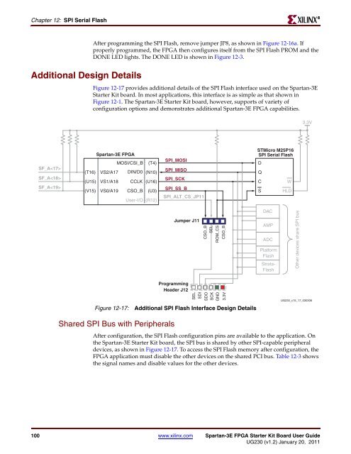
After programming the SPI Flash, remove jumper JP8, as shown in Figure 12-16a. If<br />
properly programmed, the <strong>FPGA</strong> then configures itself from the SPI Flash PROM and the<br />
DONE LED lights. The DONE LED is shown in Figure 12-3.<br />
Figure 12-17 provides additional details of the SPI Flash interface used on the <strong>Spartan</strong>-<strong>3E</strong><br />
<strong>Starter</strong> <strong>Kit</strong> board. In most applications, this interface is as simple as that shown in<br />
Figure 12-1. The <strong>Spartan</strong>-<strong>3E</strong> <strong>Starter</strong> <strong>Kit</strong> board, however, supports of variety of<br />
configuration options and demonstrates additional <strong>Spartan</strong>-<strong>3E</strong> <strong>FPGA</strong> capabilities.<br />
<strong>Spartan</strong>-<strong>3E</strong> <strong>FPGA</strong><br />
MOSI/CSI_B (T4)<br />
VS2/A17 DIN/D0 (N10)<br />
VS1/A18<br />
VS0/A19<br />
CCLK<br />
CSO_B<br />
(U16)<br />
(U3)<br />
<strong>User</strong>-I/O (R12)<br />
Figure 12-17: Additional SPI Flash Interface Design Details<br />
Shared SPI Bus with Peripherals<br />
SPI_MOSI<br />
SPI_MISO<br />
SPI_SCK<br />
SPI_SS_B<br />
SPI_ALT_CS_JP11<br />
Jumper J11<br />
Programming<br />
Header J12<br />
CSO_B<br />
SEL<br />
ROM_CS<br />
CSO_B<br />
SEL<br />
SDI<br />
SDO<br />
SCK<br />
GND<br />
3.3V<br />
STMicro M25P16<br />
SPI Serial Flash<br />
D<br />
After configuration, the SPI Flash configuration pins are available to the application. On<br />
the <strong>Spartan</strong>-<strong>3E</strong> <strong>Starter</strong> <strong>Kit</strong> board, the SPI bus is shared by other SPI-capable peripheral<br />
devices, as shown in Figure 12-17. To access the SPI Flash memory after configuration, the<br />
<strong>FPGA</strong> application must disable the other devices on the shared PCI bus. Table 12-3 shows<br />
the signal names and disable values for the other devices.<br />
100 www.xilinx.com <strong>Spartan</strong>-<strong>3E</strong> <strong>FPGA</strong> <strong>Starter</strong> <strong>Kit</strong> <strong>Board</strong> <strong>User</strong> <strong>Guide</strong><br />
<strong>UG230</strong> (v1.2) January 20, 2011<br />
Q<br />
C<br />
S<br />
DAC<br />
AMP<br />
ADC<br />
Platform<br />
Flash<br />
Strata-<br />
Flash<br />
W<br />
HLD<br />
Other devices share SPI bus<br />
3.3V<br />
<strong>UG230</strong>_c15_17_030306<br />
R