Xilinx UG230 Spartan-3E FPGA Starter Kit Board User Guide
Xilinx UG230 Spartan-3E FPGA Starter Kit Board User Guide
Xilinx UG230 Spartan-3E FPGA Starter Kit Board User Guide

You also want an ePaper? Increase the reach of your titles
YUMPU automatically turns print PDFs into web optimized ePapers that Google loves.
R<br />
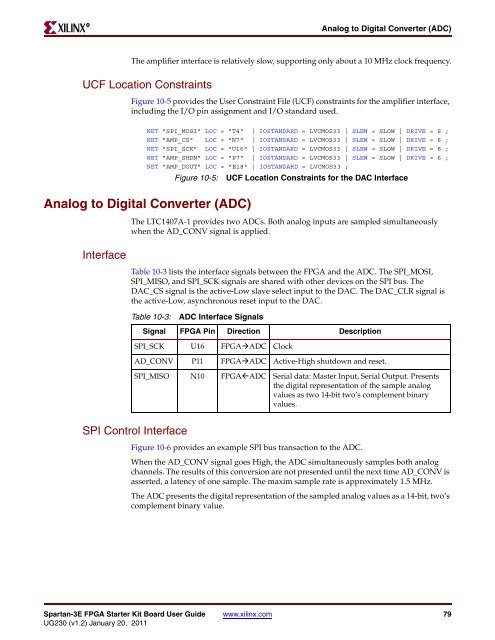
Analog to Digital Converter (ADC)<br />
The amplifier interface is relatively slow, supporting only about a 10 MHz clock frequency.<br />
UCF Location Constraints<br />
Figure 10-5 provides the <strong>User</strong> Constraint File (UCF) constraints for the amplifier interface,<br />
including the I/O pin assignment and I/O standard used.<br />
Analog to Digital Converter (ADC)<br />
Interface<br />
The LTC1407A-1 provides two ADCs. Both analog inputs are sampled simultaneously<br />
when the AD_CONV signal is applied.<br />
Table 10-3 lists the interface signals between the <strong>FPGA</strong> and the ADC. The SPI_MOSI,<br />
SPI_MISO, and SPI_SCK signals are shared with other devices on the SPI bus. The<br />
DAC_CS signal is the active-Low slave select input to the DAC. The DAC_CLR signal is<br />
the active-Low, asynchronous reset input to the DAC.<br />
SPI Control Interface<br />
NET "SPI_MOSI" LOC = "T4" | IOSTANDARD = LVCMOS33 | SLEW = SLOW | DRIVE = 6 ;<br />
NET "AMP_CS" LOC = "N7" | IOSTANDARD = LVCMOS33 | SLEW = SLOW | DRIVE = 6 ;<br />
NET "SPI_SCK" LOC = "U16" | IOSTANDARD = LVCMOS33 | SLEW = SLOW | DRIVE = 8 ;<br />
NET "AMP_SHDN" LOC = "P7" | IOSTANDARD = LVCMOS33 | SLEW = SLOW | DRIVE = 6 ;<br />
NET "AMP_DOUT" LOC = "E18" | IOSTANDARD = LVCMOS33 ;<br />
Figure 10-5: UCF Location Constraints for the DAC Interface<br />
Table 10-3: ADC Interface Signals<br />
Signal <strong>FPGA</strong> Pin Direction Description<br />
SPI_SCK U16 <strong>FPGA</strong>ADC Clock<br />
AD_CONV P11 <strong>FPGA</strong>ADC Active-High shutdown and reset.<br />
SPI_MISO N10 <strong>FPGA</strong>ADC Serial data: Master Input, Serial Output. Presents<br />
the digital representation of the sample analog<br />
values as two 14-bit two’s complement binary<br />
values.<br />
Figure 10-6 provides an example SPI bus transaction to the ADC.<br />
When the AD_CONV signal goes High, the ADC simultaneously samples both analog<br />
channels. The results of this conversion are not presented until the next time AD_CONV is<br />
asserted, a latency of one sample. The maxim sample rate is approximately 1.5 MHz.<br />
The ADC presents the digital representation of the sampled analog values as a 14-bit, two’s<br />
complement binary value.<br />
<strong>Spartan</strong>-<strong>3E</strong> <strong>FPGA</strong> <strong>Starter</strong> <strong>Kit</strong> <strong>Board</strong> <strong>User</strong> <strong>Guide</strong> www.xilinx.com 79<br />
<strong>UG230</strong> (v1.2) January 20, 2011