Xilinx UG230 Spartan-3E FPGA Starter Kit Board User Guide
Xilinx UG230 Spartan-3E FPGA Starter Kit Board User Guide
Xilinx UG230 Spartan-3E FPGA Starter Kit Board User Guide

You also want an ePaper? Increase the reach of your titles
YUMPU automatically turns print PDFs into web optimized ePapers that Google loves.
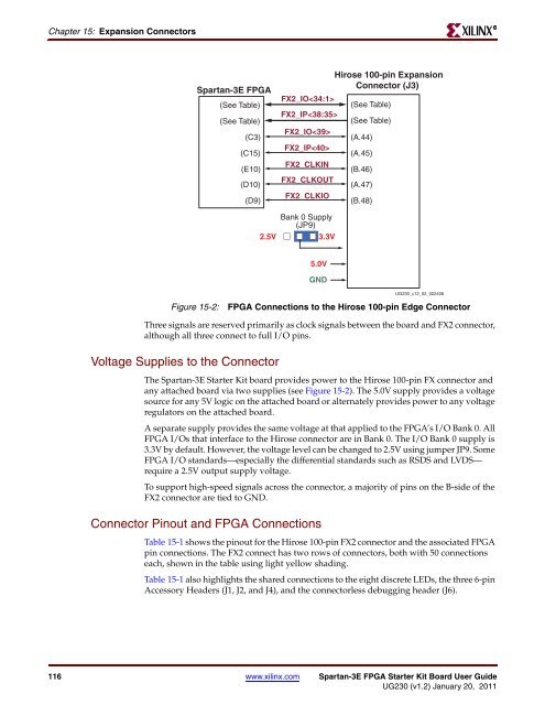
Chapter 15: Expansion Connectors<br />
<strong>Spartan</strong>-<strong>3E</strong> <strong>FPGA</strong><br />
(See Table)<br />
(See Table)<br />
(C3)<br />
(C15)<br />
(E10)<br />
(D10)<br />
(D9)<br />
Figure 15-2: <strong>FPGA</strong> Connections to the Hirose 100-pin Edge Connector<br />
Three signals are reserved primarily as clock signals between the board and FX2 connector,<br />
although all three connect to full I/O pins.<br />
Voltage Supplies to the Connector<br />
FX2_IO<br />
FX2_IP<br />
FX2_IO<br />
FX2_IP<br />
FX2_CLKIN<br />
FX2_CLKOUT<br />
FX2_CLKIO<br />
Bank 0 Supply<br />
(JP9)<br />
2.5V<br />
3.3V<br />
The <strong>Spartan</strong>-<strong>3E</strong> <strong>Starter</strong> <strong>Kit</strong> board provides power to the Hirose 100-pin FX connector and<br />
any attached board via two supplies (see Figure 15-2). The 5.0V supply provides a voltage<br />
source for any 5V logic on the attached board or alternately provides power to any voltage<br />
regulators on the attached board.<br />
A separate supply provides the same voltage at that applied to the <strong>FPGA</strong>’s I/O Bank 0. All<br />
<strong>FPGA</strong> I/Os that interface to the Hirose connector are in Bank 0. The I/O Bank 0 supply is<br />
3.3V by default. However, the voltage level can be changed to 2.5V using jumper JP9. Some<br />
<strong>FPGA</strong> I/O standards—especially the differential standards such as RSDS and LVDS—<br />
require a 2.5V output supply voltage.<br />
To support high-speed signals across the connector, a majority of pins on the B-side of the<br />
FX2 connector are tied to GND.<br />
Connector Pinout and <strong>FPGA</strong> Connections<br />
Hirose 100-pin Expansion<br />
Connector (J3)<br />
Table 15-1 shows the pinout for the Hirose 100-pin FX2 connector and the associated <strong>FPGA</strong><br />
pin connections. The FX2 connect has two rows of connectors, both with 50 connections<br />
each, shown in the table using light yellow shading.<br />
Table 15-1 also highlights the shared connections to the eight discrete LEDs, the three 6-pin<br />
Accessory Headers (J1, J2, and J4), and the connectorless debugging header (J6).<br />
116 www.xilinx.com <strong>Spartan</strong>-<strong>3E</strong> <strong>FPGA</strong> <strong>Starter</strong> <strong>Kit</strong> <strong>Board</strong> <strong>User</strong> <strong>Guide</strong><br />
<strong>UG230</strong> (v1.2) January 20, 2011<br />
5.0V<br />
GND<br />
(See Table)<br />
(See Table)<br />
(A.44)<br />
(A.45)<br />
(B.46)<br />
(A.47)<br />
(B.48)<br />
<strong>UG230</strong>_c12_02_022406<br />
R