Xilinx UG230 Spartan-3E FPGA Starter Kit Board User Guide
Xilinx UG230 Spartan-3E FPGA Starter Kit Board User Guide
Xilinx UG230 Spartan-3E FPGA Starter Kit Board User Guide

Create successful ePaper yourself
Turn your PDF publications into a flip-book with our unique Google optimized e-Paper software.
Chapter 9: Digital to Analog Converter (DAC)<br />
Interface Signals<br />
<strong>Spartan</strong>-<strong>3E</strong> <strong>FPGA</strong><br />
3.3V<br />
2.5V<br />
(N10) (T4)<br />
SPI_MOSI<br />
(N8)<br />
DAC_CS<br />
(U16)<br />
SPI_SCK<br />
(P8)<br />
DAC_CLR<br />
SPI_MISO<br />
DAC A<br />
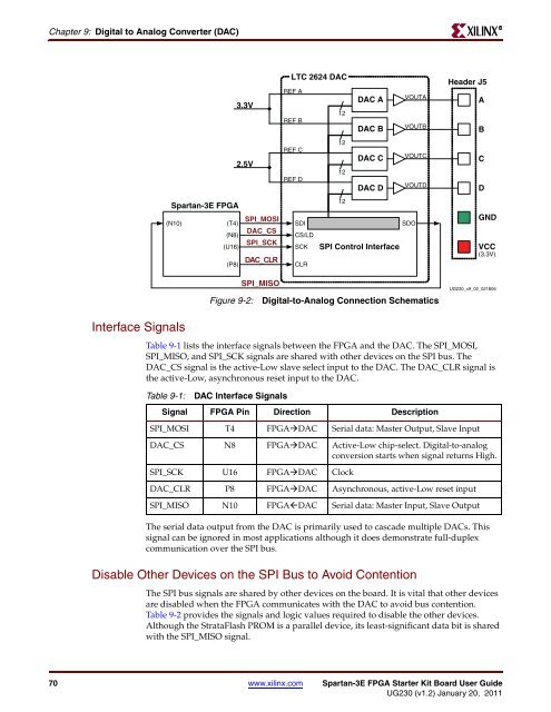
Figure 9-2: Digital-to-Analog Connection Schematics<br />
Table 9-1 lists the interface signals between the <strong>FPGA</strong> and the DAC. The SPI_MOSI,<br />
SPI_MISO, and SPI_SCK signals are shared with other devices on the SPI bus. The<br />
DAC_CS signal is the active-Low slave select input to the DAC. The DAC_CLR signal is<br />
the active-Low, asynchronous reset input to the DAC.<br />
Table 9-1: DAC Interface Signals<br />
LTC 2624 DAC<br />
The serial data output from the DAC is primarily used to cascade multiple DACs. This<br />
signal can be ignored in most applications although it does demonstrate full-duplex<br />
communication over the SPI bus.<br />
Disable Other Devices on the SPI Bus to Avoid Contention<br />
Header J5<br />
The SPI bus signals are shared by other devices on the board. It is vital that other devices<br />
are disabled when the <strong>FPGA</strong> communicates with the DAC to avoid bus contention.<br />
Table 9-2 provides the signals and logic values required to disable the other devices.<br />
Although the StrataFlash PROM is a parallel device, its least-significant data bit is shared<br />
with the SPI_MISO signal.<br />
70 www.xilinx.com <strong>Spartan</strong>-<strong>3E</strong> <strong>FPGA</strong> <strong>Starter</strong> <strong>Kit</strong> <strong>Board</strong> <strong>User</strong> <strong>Guide</strong><br />
<strong>UG230</strong> (v1.2) January 20, 2011<br />
REF A<br />
REF B<br />
REF C<br />
REF D<br />
SDI<br />
CS/LD<br />
SCK<br />
CLR<br />
12<br />
12<br />
12<br />
12<br />
DAC B<br />
DAC C<br />
DAC D<br />
SPI Control Interface<br />
VOUTA<br />
VOUTB<br />
VOUTC<br />
VOUTD<br />
Signal <strong>FPGA</strong> Pin Direction Description<br />
SDO<br />
A<br />
B<br />
C<br />
D<br />
GND<br />
VCC<br />
(3.3V)<br />
<strong>UG230</strong>_c9_02_021806<br />
SPI_MOSI T4 <strong>FPGA</strong>DAC Serial data: Master Output, Slave Input<br />
DAC_CS N8 <strong>FPGA</strong>DAC Active-Low chip-select. Digital-to-analog<br />
conversion starts when signal returns High.<br />
SPI_SCK U16 <strong>FPGA</strong>DAC Clock<br />
DAC_CLR P8 <strong>FPGA</strong>DAC Asynchronous, active-Low reset input<br />
SPI_MISO N10 <strong>FPGA</strong>DAC Serial data: Master Input, Slave Output<br />
R