Xilinx UG230 Spartan-3E FPGA Starter Kit Board User Guide
Xilinx UG230 Spartan-3E FPGA Starter Kit Board User Guide
Xilinx UG230 Spartan-3E FPGA Starter Kit Board User Guide

Create successful ePaper yourself
Turn your PDF publications into a flip-book with our unique Google optimized e-Paper software.
R<br />
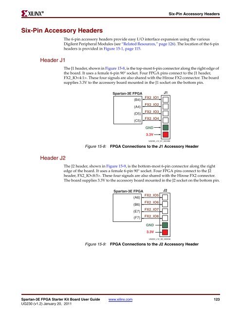
Six-Pin Accessory Headers<br />
Header J1<br />
Header J2<br />
Six-Pin Accessory Headers<br />
The 6-pin accessory headers provide easy I/O interface expansion using the various<br />
Digilent Peripheral Modules (see “Related Resources,” page 126). The location of the 6-pin<br />
headers is provided in Figure 15-1, page 115.<br />
The J1 header, shown in Figure 15-8, is the top-most 6-pin connector along the right edge of<br />
the board. It uses a female 6-pin 90° socket. Four <strong>FPGA</strong> pins connect to the J1 header,<br />
FX2_IO. These four signals are also shared with the Hirose FX2 connector. The board<br />
supplies 3.3V to the accessory board mounted in the J1 socket on the bottom pin.<br />
(B4) FX2_IO1<br />
<strong>Spartan</strong>-<strong>3E</strong> <strong>FPGA</strong><br />
(A4) FX2_IO2<br />
(D5) FX2_IO3<br />
(C5) FX2_IO4<br />
Figure 15-8: <strong>FPGA</strong> Connections to the J1 Accessory Header<br />
The J2 header, shown in Figure 15-9, is the bottom-most 6-pin connector along the right<br />
edge of the board. It uses a female 6-pin 90° socket. Four <strong>FPGA</strong> pins connect to the J2<br />
header, FX2_IO. These four signals are also shared with the Hirose FX2 connector.<br />
The board supplies 3.3V to the accessory board mounted in the J2 socket on the bottom pin.<br />
<strong>Spartan</strong>-<strong>3E</strong> <strong>FPGA</strong> <strong>Starter</strong> <strong>Kit</strong> <strong>Board</strong> <strong>User</strong> <strong>Guide</strong> www.xilinx.com 123<br />
<strong>UG230</strong> (v1.2) January 20, 2011<br />
GND<br />
3.3V<br />
J1<br />
<strong>UG230</strong>_c12_07_022406<br />
<strong>Spartan</strong>-<strong>3E</strong> <strong>FPGA</strong><br />
(A6)<br />
FX2_IO5<br />
(B6)<br />
FX2_IO6<br />
(E7)<br />
FX2_IO7<br />
(F7) FX2_IO8<br />
GND<br />
3.3V<br />
Figure 15-9: <strong>FPGA</strong> Connections to the J2 Accessory Header<br />
J2<br />
<strong>UG230</strong>_c12_08_022406