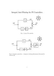
Predictive Control of Three Phase AC/DC Converters
Predictive Control of Three Phase AC/DC Converters
Predictive Control of Three Phase AC/DC Converters

Create successful ePaper yourself
Turn your PDF publications into a flip-book with our unique Google optimized e-Paper software.
010UP3<br />
β<br />
23<br />
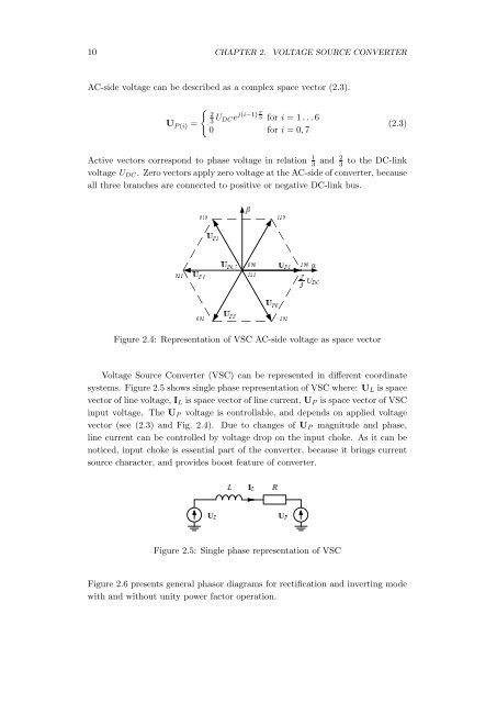
Figure 2.4: Representation <strong>of</strong> VSC <strong>AC</strong>-side voltage as space vector<br />
111<br />
110<br />
10 CHAPTER 2. VOLTAGE SOURCE CONVERTER<br />
<strong>AC</strong>-side voltage can be described as a complex space vector (2.3).<br />
U P (i) =<br />
{<br />
2<br />
3 U <strong>DC</strong> e j(i−1) π 3 for i = 1 . . . 6<br />
0 for i = 0, 7<br />
(2.3)<br />
Active vectors correspond to phase voltage in relation 1 3 and 2 3<br />
to the <strong>DC</strong>-link<br />
voltage U <strong>DC</strong> . Zero vectors apply zero voltage at the <strong>AC</strong>-side <strong>of</strong> converter, because<br />
all three branches are connected to positive or negative <strong>DC</strong>-link bus.<br />
011<br />
UP1 U<strong>DC</strong> UP4 α UP6 UP0,7 100 000<br />
UP5<br />
001<br />
Voltage Source Converter (VSC) can be represented in different coordinate<br />
systems. Figure 2.5 shows single phase representation <strong>of</strong> VSC where: U L is space<br />
vector <strong>of</strong> line voltage, I L is space vector <strong>of</strong> line current, U<br />
101<br />
P is space vector <strong>of</strong> VSC<br />
input voltage. The U P voltage is controllable, and depends on applied voltage<br />
vector (see (2.3) and Fig. 2.4). Due to changes <strong>of</strong> U P magnitude and phase,<br />
line current can be controlled by voltage drop on the input choke. As it can be<br />
noticed, input choke is essential part <strong>of</strong> the converter, because it brings current<br />
source character, and provides boost feature <strong>of</strong> converter.<br />
Figure 2.5: Single phase representation <strong>of</strong> VSC<br />
R<br />
IL UP<br />
Figure 2.6 presents general phasor diagrams for rectification and inverting mode<br />
with and without unity power factor operation.<br />
ULL


![[TCP] Opis układu - Instytut Sterowania i Elektroniki Przemysłowej ...](https://img.yumpu.com/23535443/1/184x260/tcp-opis-ukladu-instytut-sterowania-i-elektroniki-przemyslowej-.jpg?quality=85)