Predictive Control of Three Phase AC/DC Converters
Predictive Control of Three Phase AC/DC Converters
Predictive Control of Three Phase AC/DC Converters

Create successful ePaper yourself
Turn your PDF publications into a flip-book with our unique Google optimized e-Paper software.
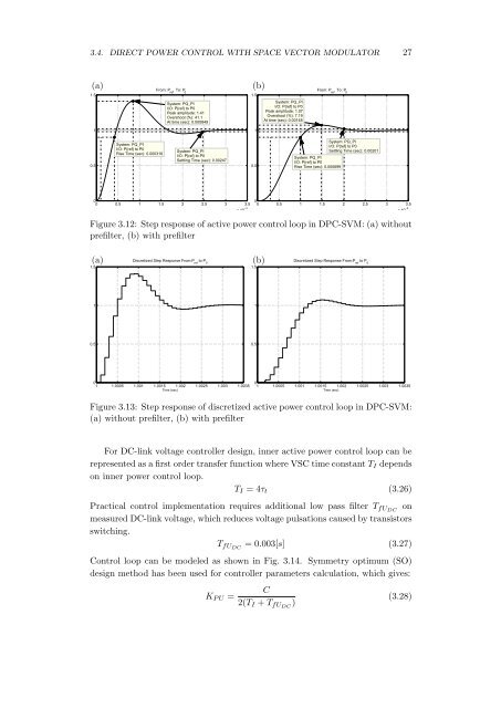
3.4. DIRECT POWER CONTROL WITH SP<strong>AC</strong>E VECTOR MODULATOR 27<br />
(a)<br />
1.5<br />
From: P ref<br />
To: P 0<br />
System: PQ_PI<br />
I/O: P{ref} to P0<br />
Peak amplitude: 1.41<br />
Overshoot (%): 41.1<br />
At time (sec): 0.000849<br />
(b)<br />
1.5<br />
System: PQ_PI<br />
I/O: P{ref} to P0<br />
Peak amplitude: 1.07<br />
Overshoot (%): 7.19<br />
At time (sec): 0.00148<br />
From: P ref<br />
To: P 0<br />
1<br />
1<br />
0.5<br />
System: PQ_PI<br />
I/O: P{ref} to P0<br />
Rise Time (sec): 0.000316<br />
System: PQ_PI<br />
I/O: P{ref} to P0<br />
Settling Time (sec): 0.00247<br />
0.5<br />
System: PQ_PI<br />
I/O: P{ref} to P0<br />
Rise Time (sec): 0.000699<br />
System: PQ_PI<br />
I/O: P{ref} to P0<br />
Settling Time (sec): 0.00201<br />
0<br />
0 0.5 1 1.5 2 2.5 3 3.5<br />
x 10 −3<br />
0<br />
0 0.5 1 1.5 2 2.5 3 3.5<br />
x 10 −3<br />
Figure 3.12: Step response <strong>of</strong> active power control loop in DPC-SVM: (a) without<br />
prefilter, (b) with prefilter<br />
(a)<br />
1.5<br />
Discretized Step Response From:P ref<br />
to P 0<br />
(b)<br />
1.5<br />
Discretized Step Response From:P ref<br />
to P 0<br />
1<br />
1<br />
0.5<br />
0.5<br />
0<br />
1 1.0005 1.001 1.0015 1.002 1.0025 1.003 1.0035<br />
Time (sec)<br />
0<br />
1 1.0005 1.001 1.0015 1.002 1.0025 1.003 1.0035<br />
Time (sec)<br />
Figure 3.13: Step response <strong>of</strong> discretized active power control loop in DPC-SVM:<br />
(a) without prefilter, (b) with prefilter<br />
For <strong>DC</strong>-link voltage controller design, inner active power control loop can be<br />
represented as a first order transfer function where VSC time constant T I depends<br />
on inner power control loop.<br />
T I = 4τ t (3.26)<br />
Practical control implementation requires additional low pass filter T fU<strong>DC</strong> on<br />
measured <strong>DC</strong>-link voltage, which reduces voltage pulsations caused by transistors<br />
switching.<br />
T fU<strong>DC</strong> = 0.003[s] (3.27)<br />
<strong>Control</strong> loop can be modeled as shown in Fig. 3.14. Symmetry optimum (SO)<br />
design method has been used for controller parameters calculation, which gives:<br />
K P U =<br />
C<br />
2(T I + T fU<strong>DC</strong> )<br />
(3.28)


![[TCP] Opis układu - Instytut Sterowania i Elektroniki Przemysłowej ...](https://img.yumpu.com/23535443/1/184x260/tcp-opis-ukladu-instytut-sterowania-i-elektroniki-przemyslowej-.jpg?quality=85)