Power Management Design Guide for Altera® FPGAs and CPLDs ...
Power Management Design Guide for Altera® FPGAs and CPLDs ...
Power Management Design Guide for Altera® FPGAs and CPLDs ...

Create successful ePaper yourself
Turn your PDF publications into a flip-book with our unique Google optimized e-Paper software.
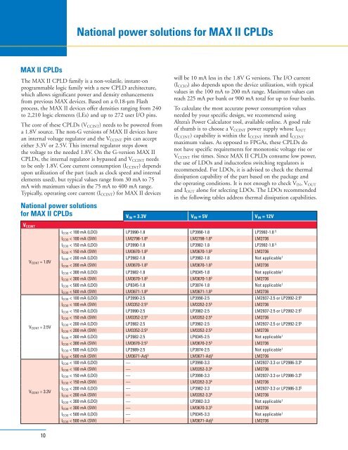
National power solutions <strong>for</strong> MAX II <strong>CPLDs</strong><br />
MAX II <strong>CPLDs</strong><br />
The MAX II CPLD family is a non-volatile, instant-on<br />
programmable logic family with a new CPLD architecture,<br />
which allows significant power <strong>and</strong> density enhancements<br />
from previous MAX devices. Based on a 0.18-µm Flash<br />
process, the MAX II devices offer densities ranging from 240<br />
to 2,210 logic elements (LEs) <strong>and</strong> up to 272 user I/O pins.<br />
The core of these <strong>CPLDs</strong> (V CCINT ) needs to be powered from<br />
a 1.8V source. The non-G versions of MAX II devices have<br />
an internal voltage regulator <strong>and</strong> the V CCINT pin can accept<br />
either 3.3V or 2.5V. This internal regulator steps down<br />
the voltage to the needed 1.8V. On the G-version MAX II<br />
<strong>CPLDs</strong>, the internal regulator is bypassed <strong>and</strong> V CCINT needs<br />
to be only 1.8V. Core current consumption (I CCINT ) depends<br />
upon utilization of the part (such as clock speed <strong>and</strong> internal<br />
elements used), but typical values range from 30 mA to 75<br />
mA with maximum values in the 75 mA to 400 mA range.<br />
Typically, operating core current (I CCINT ) <strong>for</strong> MAX II devices<br />
National power solutions<br />
<strong>for</strong> MAX II <strong>CPLDs</strong><br />
will be 10 mA less in the 1.8V G versions. The I/O current<br />
(I CCIO ) also depends upon the device utilization, with typical<br />
values in the 100 mA to 200 mA range. Maximum values can<br />
reach 225 mA per bank or 900 mA total <strong>for</strong> up to four banks.<br />
To calculate the most accurate power consumption values<br />
needed by your specific design, we recommend using<br />
Altera’s <strong>Power</strong> Calculator tool, available online. A good rule<br />
of thumb is to choose a V CCINT power supply whose I OUT<br />
(I CCINT ) capability is within the I CCINT inrush <strong>and</strong> I CCINT<br />
maximum values. As opposed to <strong>FPGAs</strong>, these <strong>CPLDs</strong> do<br />
not have specific requirements <strong>for</strong> monotonic voltage rise or<br />
V CCINT rise times. Since MAX II <strong>CPLDs</strong> consume low power,<br />
the use of LDOs <strong>and</strong> inductorless switching regulators is<br />
recommended. For LDOs, it is advised to check the thermal<br />
dissipation capability of the part based on the package <strong>and</strong><br />
the operating conditions. It is not enough to check V IN , V OUT<br />
<strong>and</strong> I OUT alone <strong>for</strong> selecting LDOs. The LDOs recommended<br />
in the following tables address thermal dissipation capabilities.<br />
V IN = 3.3V V IN = 5V V IN = 12V<br />
V CCINT<br />
V CCINT = 1.8V<br />
V CCINT = 2.5V<br />
V CCINT = 3.3V<br />
I CCIO < 100 mA (LDO) LP3990-1.8 LP3990-1.8 LP2992-1.8 5<br />
I CCIO < 100 mA (SW) LM2798-1.8 4 LM2798-1.8 4 LM2736<br />
I CCIO < 150 mA (LDO) LP3990-1.8 LP3982-1.8 LP2992-1.8 5<br />
I CCIO < 150 mA (SW) LM3670-1.8 3 LM3670-1.8 3 LM2736<br />
I CCIO < 200 mA (LDO) LP3982-1.8 LP3982-1.8 Not applicable 1<br />
I CCIO < 200 mA (SW) LM3670-1.8 3 LM3670-1.8 3 LM2736<br />
I CCIO < 300 mA (LDO) LP3982-1.8 LP8345-1.8 Not applicable 1<br />
I CCIO < 300 mA (SW) LM3670-1.8 3 LM3670-1.8 3 LM2736<br />
I CCIO < 500 mA (LDO) LP8345-1.8 LP3874-1.8 Not applicable 1<br />
I CCIO < 500 mA (SW) LM3671-1.8 3 LM3671-1.8 3 LM2736<br />
I CCIO < 100 mA (LDO) LP3990-2.5 LP3990-2.5 LM2937-2.5 or LP2992-2.5 5<br />
I CCIO < 100 mA (SW) LM3352-2.5 4 LM3352-2.5 4 LM2736<br />
I CCIO < 150 mA (LDO) LP3990-2.5 LP3982-2.5 LM2937-2.5 or LP2992-2.5 5<br />
I CCIO < 150 mA (SW) LM3352-2.5 4 LM3352-2.5 4 LM2736<br />
I CCIO < 200 mA (LDO) LP3982-2.5 LP3982-2.5 LM2937-2.5 or LP2992-2.5 5<br />
I CCIO < 200 mA (SW) LM3352-2.5 4 LM3352-2.5 4 LM2736<br />
I CCIO < 300 mA (LDO) LP3982-2.5 LP8345-2.5 Not applicable 1<br />
I CCIO < 300 mA (SW) LM3670-2.5 3 LM3670-2.5 3 LM2736<br />
I CCIO < 500 mA (LDO) LP2989-2.5 LP3874-2.5 Not applicable 1<br />
I CCIO < 500 mA (SW) LM3671-Adj 3 LM3671-Adj 3 LM2736<br />
I CCIO < 100 mA (LDO) — LP3990-3.3 LM2937-3.3 or LP2986-3.3 5<br />
I CCIO < 100 mA (SW) — LM3352-3.3 4 LM2736<br />
I CCIO < 150 mA (LDO) — LP3990-3.3 LM2937-3.3 or LP2986-3.3 5<br />
I CCIO < 150 mA (SW) — LM3352-3.3 4 LM2736<br />
I CCIO < 200 mA (LDO) — LP3982-3.3 LM2937-3.3 or LP2986-3.3 5<br />
I CCIO < 200 mA (SW) — LM3352-3.3 4 LM2736<br />
I CCIO < 300 mA (LDO) — LP3982-3.3 Not applicable 1<br />
I CCIO < 300 mA (SW) — LM3670-3.3 3 LM2736<br />
I CCIO < 500 mA (LDO) — LP8345-3.3 Not applicable 1<br />
I CCIO < 500 mA (SW) — LM3671-Adj 3 LM2736<br />
10