Power Management Design Guide for Altera® FPGAs and CPLDs ...
Power Management Design Guide for Altera® FPGAs and CPLDs ...
Power Management Design Guide for Altera® FPGAs and CPLDs ...

You also want an ePaper? Increase the reach of your titles
YUMPU automatically turns print PDFs into web optimized ePapers that Google loves.
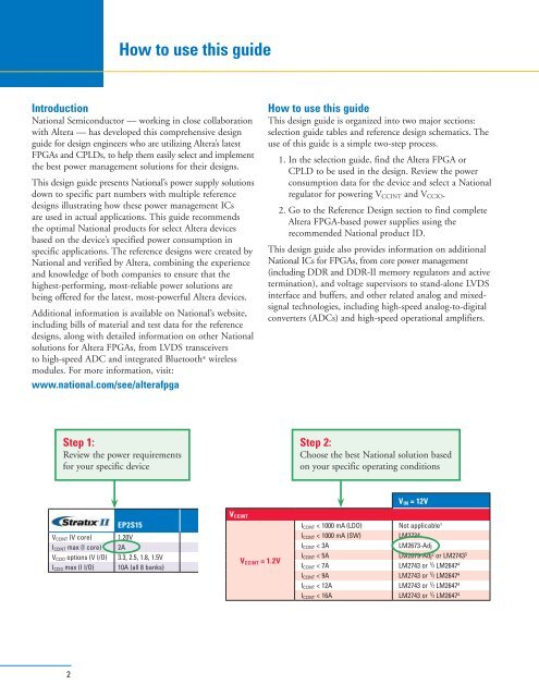
How to use this guide<br />
Introduction<br />
National Semiconductor — working in close collaboration<br />
with Altera — has developed this comprehensive design<br />
guide <strong>for</strong> design engineers who are utilizing Altera’s latest<br />
<strong>FPGAs</strong> <strong>and</strong> <strong>CPLDs</strong>, to help them easily select <strong>and</strong> implement<br />
the best power management solutions <strong>for</strong> their designs.<br />
This design guide presents National’s power supply solutions<br />
down to specific part numbers with multiple reference<br />
designs illustrating how these power management ICs<br />
are used in actual applications. This guide recommends<br />
the optimal National products <strong>for</strong> select Altera devices<br />
based on the device’s specified power consumption in<br />
specific applications. The reference designs were created by<br />
National <strong>and</strong> verified by Altera, combining the experience<br />
<strong>and</strong> knowledge of both companies to ensure that the<br />
highest-per<strong>for</strong>ming, most-reliable power solutions are<br />
being offered <strong>for</strong> the latest, most-powerful Altera devices.<br />
Additional in<strong>for</strong>mation is available on National’s website,<br />
including bills of material <strong>and</strong> test data <strong>for</strong> the reference<br />
designs, along with detailed in<strong>for</strong>mation on other National<br />
solutions <strong>for</strong> Altera <strong>FPGAs</strong>, from LVDS transceivers<br />
to high-speed ADC <strong>and</strong> integrated Bluetooth ® wireless<br />
modules. For more in<strong>for</strong>mation, visit:<br />
www.national.com/see/alterafpga<br />
How to use this guide<br />
This design guide is organized into two major sections:<br />
selection guide tables <strong>and</strong> reference design schematics. The<br />
use of this guide is a simple two-step process.<br />
1. In the selection guide, find the Altera FPGA or<br />
CPLD to be used in the design. Review the power<br />
consumption data <strong>for</strong> the device <strong>and</strong> select a National<br />
regulator <strong>for</strong> powering V CCINT <strong>and</strong> V CCIO .<br />
2. Go to the Reference <strong>Design</strong> section to find complete<br />
Altera FPGA-based power supplies using the<br />
recommended National product ID.<br />
This design guide also provides in<strong>for</strong>mation on additional<br />
National ICs <strong>for</strong> <strong>FPGAs</strong>, from core power management<br />
(including DDR <strong>and</strong> DDR-II memory regulators <strong>and</strong> active<br />
termination), <strong>and</strong> voltage supervisors to st<strong>and</strong>-alone LVDS<br />
interface <strong>and</strong> buffers, <strong>and</strong> other related analog <strong>and</strong> mixedsignal<br />
technologies, including high-speed analog-to-digital<br />
converters (ADCs) <strong>and</strong> high-speed operational amplifiers.<br />
Step 1:<br />
Review the power requirements<br />
<strong>for</strong> your specific device<br />
Step 2:<br />
Choose the best National solution based<br />
on your specific operating conditions<br />
EP2S15<br />
V CCINT (V core) 1.20V<br />
I CCINT max (I core) 2A<br />
V CCIO options (V I/O) 3.3, 2.5, 1.8, 1.5V<br />
I CCIO max (I I/O) 10A (all 8 banks)<br />
V CCINT<br />
V CCINT = 1.2V<br />
V IN = 12V<br />
I CCINT < 1000 mA (LDO) Not applicable 1<br />
I CCINT < 1000 mA (SW)<br />
LM2734<br />
I CCINT < 3A<br />
LM2673-Adj<br />
I CCINT < 5A LM2679-Adj 2 or LM2743 3<br />
I CCINT < 7A LM2743 or 1 / 2 LM2647 4<br />
I CCINT < 9A LM2743 or 1 / 2 LM2647 4<br />
I CCINT < 12A LM2743 or 1 / 2 LM2647 4<br />
I CCINT < 16A LM2743 or 1 / 2 LM2647 4<br />
2