Power Management Design Guide for Altera® FPGAs and CPLDs ...
Power Management Design Guide for Altera® FPGAs and CPLDs ...
Power Management Design Guide for Altera® FPGAs and CPLDs ...

You also want an ePaper? Increase the reach of your titles
YUMPU automatically turns print PDFs into web optimized ePapers that Google loves.
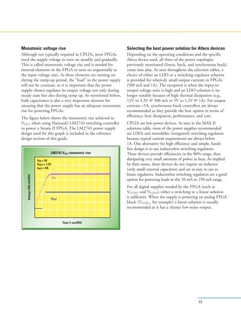
Monotonic voltage rise<br />
Although not typically required in <strong>CPLDs</strong>, most <strong>FPGAs</strong><br />
need the supply voltage to turn on steadily <strong>and</strong> gradually.<br />
This is called monotonic voltage rise <strong>and</strong> is needed <strong>for</strong><br />
internal elements in the FPGA to turn on sequentially as<br />
the input voltage rises. As these elements are turning on<br />
during the ramp-up period, the “load” to the power supply<br />
will not be constant, so it is important that the power<br />
supply chosen regulates its output voltage not only during<br />
steady state but also during ramp up. As mentioned be<strong>for</strong>e,<br />
bulk capacitance is also a very important element <strong>for</strong><br />
ensuring that the power supply has an adequate monotonic<br />
rise <strong>for</strong> powering <strong>FPGAs</strong>.<br />
The figure below shows the monotonic rise achieved in<br />
V OUT when using National’s LM2743 switching controller<br />
to power a Stratix II FPGA. The LM2743 power supply<br />
design used <strong>for</strong> this graph is included in the reference<br />
design section of this guide.<br />
<br />
<br />
<br />
<br />
LM2743 V OUT monotonic rise<br />
<br />
<br />
Selecting the best power solution <strong>for</strong> Altera devices<br />
Depending on the operating conditions <strong>and</strong> the specific<br />
Altera device used, all three of the power topologies<br />
previously mentioned (linear, buck, <strong>and</strong> synchronous buck)<br />
come into play. As seen throughout the selection tables, a<br />
choice of either an LDO or a switching regulator solution<br />
is provided <strong>for</strong> relatively small output currents in <strong>FPGAs</strong><br />
(500 mA <strong>and</strong> 1A). The exception is when the input-tooutput<br />
voltage ratio is high <strong>and</strong> an LDO solution is no<br />
longer suitable because of high thermal dissipation (e.g.,<br />
12V to 3.3V @ 500 mA or 5V to 1.2V @ 1A). For output<br />
currents >5A, synchronous buck controllers are always<br />
recommended as they provide the best option in terms of<br />
efficiency, heat dissipation, per<strong>for</strong>mance, <strong>and</strong> cost.<br />
<strong>CPLDs</strong> are low-power devices. As seen in the MAX II<br />
solutions table, most of the power supplies recommended<br />
are LDOs <strong>and</strong> monolithic (integrated) switching regulators<br />
because typical current requirements are always below<br />
1A. One alternative <strong>for</strong> high efficiency <strong>and</strong> simple, hasslefree<br />
design is to use inductorless switching regulators.<br />
These devices provide efficiencies in the 80% range, thus<br />
dissipating very small amounts of power as heat. As implied<br />
by their name, these devices do not require an inductor<br />
(only small external capacitors) <strong>and</strong> are as easy to use as<br />
linear regulators. Inductorless switching regulators are a good<br />
option <strong>for</strong> powering loads in the 10 mA to 250 mA range.<br />
For all digital supplies needed by the FPGA (such as<br />
V CCINT <strong>and</strong> V CCIO ), either a switching or a linear solution<br />
is sufficient. When the supply is powering an analog FPGA<br />
block (V CCPLL , <strong>for</strong> example) a linear solution is usually<br />
recommended as it has a cleaner low-noise output.<br />
<br />
13