Power Management Design Guide for Altera® FPGAs and CPLDs ...
Power Management Design Guide for Altera® FPGAs and CPLDs ...
Power Management Design Guide for Altera® FPGAs and CPLDs ...

You also want an ePaper? Increase the reach of your titles
YUMPU automatically turns print PDFs into web optimized ePapers that Google loves.
National power solutions <strong>for</strong> Stratix <strong>FPGAs</strong><br />
Stratix <strong>FPGAs</strong><br />
The Stratix FPGA family is optimized to address the<br />
challenges of high-b<strong>and</strong>width systems. Stratix devices offer<br />
very high core per<strong>for</strong>mance, memory capacity, architectural<br />
efficiencies, <strong>and</strong> time-to-market advantages. Stratix devices<br />
offer dedicated functionality <strong>for</strong> clock management <strong>and</strong><br />
digital signal processing (DSP) applications, as well as<br />
support <strong>for</strong> differential <strong>and</strong> single-ended I/O st<strong>and</strong>ards.<br />
In addition, Stratix devices offer on-chip termination <strong>and</strong><br />
remote system upgrade capabilities.<br />
Based on a 1.5V, 0.13-µm, all-layer copper SRAM process,<br />
Stratix devices are available in densities ranging from<br />
10,570 to 79,040 logic elements (LEs) <strong>and</strong> up to 7 Mbits<br />
of RAM. Stratix devices offer up to 22 DSP blocks with<br />
up to 176 (9-bit x 9-bit) embedded multipliers, optimized<br />
complex applications that require high data throughput.<br />
The core of these <strong>FPGAs</strong> needs to be powered from a 1.5V<br />
source. Core current consumption (I CCINT ) depends upon<br />
utilization of the part (such as clock speed <strong>and</strong> internal<br />
elements used), but maximum values range from 1.5A to<br />
10A (approx.) depending on the specific Stratix device<br />
used. To calculate the most accurate power consumption<br />
values needed by a specific design, use Altera’s <strong>Power</strong><br />
Calculator tool (see www.national.com/see/alterafpga). As<br />
a general rule, choose a V CCINT power supply whose I OUT<br />
(I CCINT ) capability is within the I CCINT inrush <strong>and</strong> I CCINT<br />
maximum values given in this guide <strong>for</strong> the specific Altera<br />
device used.<br />
Another power management consideration that needs<br />
to be addressed is the monotonic rise of V CCINT . This<br />
consideration is critical <strong>for</strong> the correct operation of the<br />
FPGA. While many power supplies take this requirement<br />
into consideration, it is recommended to further support<br />
this requirement by the use of adequate bulk capacitance<br />
in the power supply.<br />
LM2647 Dual synchronous buck controller<br />
• Input voltage range from 5.5V to 28V<br />
• Synchronous dual-channel interleaved<br />
switching<br />
• PWM or pulse-skip modes<br />
• Low-side MOSFET current sensing<br />
• Adjustable output voltage down to 0.6V<br />
• <strong>Power</strong>-good flag <strong>and</strong> chip enable<br />
• Under-voltage lockout hysteresis<br />
• Over-voltage/under-voltage protection<br />
• Softstart <strong>and</strong> soft-shutdown<br />
• Switching frequency adjustable from<br />
200 kHz to 500 kHz<br />
• Available in TSSOP-28 <strong>and</strong> tiny,<br />
thermally enhanced LLP-28 packaging<br />
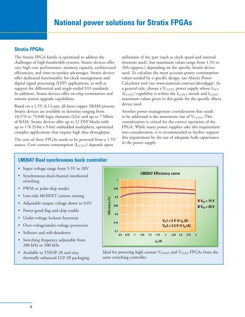
LM2647 Efficiency curve<br />
Ideal <strong>for</strong> powering high-current V CCINT <strong>and</strong> V CCIO <strong>FPGAs</strong> from the<br />
same switching controller<br />
6