Power Management Design Guide for Altera® FPGAs and CPLDs ...
Power Management Design Guide for Altera® FPGAs and CPLDs ...
Power Management Design Guide for Altera® FPGAs and CPLDs ...

You also want an ePaper? Increase the reach of your titles
YUMPU automatically turns print PDFs into web optimized ePapers that Google loves.
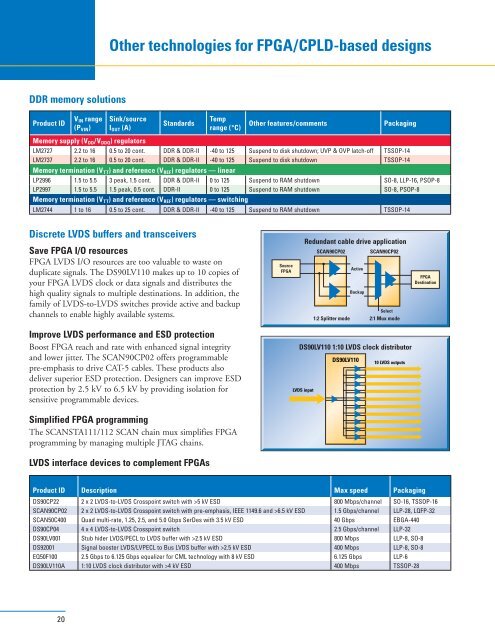
Other technologies <strong>for</strong> FPGA/CPLD-based designs<br />
DDR memory solutions<br />
Product ID<br />
V IN range<br />
(P VIN )<br />
Sink/source<br />
I OUT (A)<br />
St<strong>and</strong>ards<br />
Temp<br />
range (°C)<br />
Other features/comments<br />
Packaging<br />
Memory supply (V DD /V DDQ ) regulators<br />
LM2727 2.2 to 16 0.5 to 20 cont. DDR & DDR-II -40 to 125 Suspend to disk shutdown; UVP & OVP latch-off TSSOP-14<br />
LM2737 2.2 to 16 0.5 to 20 cont. DDR & DDR-II -40 to 125 Suspend to disk shutdown TSSOP-14<br />
Memory termination (V TT ) <strong>and</strong> reference (V REF ) regulators — linear<br />
LP2996 1.5 to 5.5 3 peak, 1.5 cont. DDR & DDR-II 0 to 125 Suspend to RAM shutdown SO-8, LLP-16, PSOP-8<br />
LP2997 1.5 to 5.5 1.5 peak, 0.5 cont. DDR-II 0 to 125 Suspend to RAM shutdown SO-8, PSOP-8<br />
Memory termination (V TT ) <strong>and</strong> reference (V REF ) regulators — switching<br />
LM2744 1 to 16 0.5 to 25 cont. DDR & DDR-II -40 to 125 Suspend to RAM shutdown TSSOP-14<br />
Discrete LVDS buffers <strong>and</strong> transceivers<br />
Save FPGA I/O resources<br />
FPGA LVDS I/O resources are too valuable to waste on<br />
duplicate signals. The DS90LV110 makes up to 10 copies of<br />
your FPGA LVDS clock or data signals <strong>and</strong> distributes the<br />
high quality signals to multiple destinations. In addition, the<br />
family of LVDS-to-LVDS switches provide active <strong>and</strong> backup<br />
channels to enable highly available systems.<br />
<br />
<br />
Redundant cable drive application<br />
<br />
<br />
<br />
<br />
<br />
<br />
<br />
Improve LVDS per<strong>for</strong>mance <strong>and</strong> ESD protection<br />
Boost FPGA reach <strong>and</strong> rate with enhanced signal integrity<br />
<strong>and</strong> lower jitter. The SCAN90CP02 offers programmable<br />
pre-emphasis to drive CAT-5 cables. These products also<br />
deliver superior ESD protection. <strong>Design</strong>ers can improve ESD<br />
protection by 2.5 kV to 6.5 kV by providing isolation <strong>for</strong><br />
sensitive programmable devices.<br />
DS90LV110 1:10 LVDS clock distributor<br />
<br />
<br />
Simplified FPGA programming<br />
The SCANSTA111/112 SCAN chain mux simplifies FPGA<br />
programming by managing multiple JTAG chains.<br />
LVDS interface devices to complement <strong>FPGAs</strong><br />
Product ID Description Max speed Packaging<br />
DS90CP22 2 x 2 LVDS-to-LVDS Crosspoint switch with >5 kV ESD 800 Mbps/channel SO-16, TSSOP-16<br />
SCAN90CP02 2 x 2 LVDS-to-LVDS Crosspoint switch with pre-emphasis, IEEE 1149.6 <strong>and</strong> >6.5 kV ESD 1.5 Gbps/channel LLP-28, LQFP-32<br />
SCAN50C400 Quad multi-rate, 1.25, 2.5, <strong>and</strong> 5.0 Gbps SerDes with 3.5 kV ESD 40 Gbps EBGA-440<br />
DS90CP04 4 x 4 LVDS-to-LVDS Crosspoint switch 2.5 Gbps/channel LLP-32<br />
DS90LV001 Stub hider LVDS/PECL to LVDS buffer with >2.5 kV ESD 800 Mbps LLP-8, SO-8<br />
DS92001 Signal booster LVDS/LVPECL to Bus LVDS buffer with >2.5 kV ESD 400 Mbps LLP-8, SO-8<br />
EQ50F100 2.5 Gbps to 6.125 Gbps equalizer <strong>for</strong> CML technology with 8 kV ESD 6.125 Gbps LLP-6<br />
DS90LV110A 1:10 LVDS clock distributor with >4 kV ESD 400 Mbps TSSOP-28<br />
20