Power Management Design Guide for Altera® FPGAs and CPLDs ...
Power Management Design Guide for Altera® FPGAs and CPLDs ...
Power Management Design Guide for Altera® FPGAs and CPLDs ...

Create successful ePaper yourself
Turn your PDF publications into a flip-book with our unique Google optimized e-Paper software.
Reference designs<br />
Stratix II & Stratix <strong>FPGAs</strong><br />
<br />
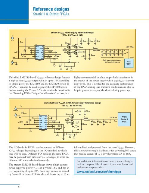
Stratix II V CCINT <strong>Power</strong> Supply Reference <strong>Design</strong><br />
(5V in, 1.20V out @ 16A)<br />
<br />
<br />
<br />
<br />
<br />
<br />
<br />
<br />
<br />
<br />
<br />
<br />
<br />
<br />
<br />
<br />
<br />
<br />
<br />
<br />
<br />
<br />
<br />
<br />
<br />
<br />
<br />
<br />
<br />
<br />
<br />
<br />
<br />
<br />
<br />
<br />
<br />
<br />
<br />
<br />
<br />
<br />
<br />
<br />
<br />
<br />
<br />
<br />
<br />
<br />
<br />
<br />
<br />
<br />
<br />
<br />
<br />
<br />
<br />
<br />
<br />
<br />
<br />
<br />
<br />
<br />
<br />
<br />
<br />
<br />
<br />
<br />
<br />
<br />
<br />
<br />
<br />
<br />
<br />
<br />
<br />
<br />
<br />
<br />
<br />
<br />
<br />
<br />
<br />
<br />
<br />
<br />
<br />
<br />
<br />
<br />
<br />
<br />
<br />
<br />
This third LM2743-based V CCINT reference design features<br />
a high-current I CCINT output with an up to 16A capability<br />
to ideally power the EP2S180 <strong>and</strong> the EP2S130 Stratix II<br />
<strong>FPGAs</strong>. It can also be used to power the EP1S80 Stratix<br />
device, making the V CCINT 1.5V. As previously described in<br />
the “<strong>Power</strong>ing FPGA <strong>Design</strong> Considerations” section, it is<br />
highly recommended to place proper bulk capacitance in<br />
the output of the power supply when large I CCINT current<br />
is involved. This is needed <strong>for</strong> the adequate per<strong>for</strong>mance<br />
of the FPGA during load transient conditions <strong>and</strong> also to<br />
help in proper start-up of the device during power up.<br />
<br />
<br />
Stratix II/Stratix V CCIO 3A to 10A <strong>Power</strong> Supply Reference <strong>Design</strong><br />
(5V in, 1.8V out @ 10A)<br />
<br />
<br />
<br />
<br />
<br />
<br />
<br />
<br />
<br />
<br />
<br />
<br />
<br />
<br />
<br />
<br />
<br />
<br />
<br />
<br />
<br />
<br />
<br />
<br />
<br />
<br />
<br />
<br />
<br />
<br />
<br />
<br />
<br />
<br />
<br />
<br />
<br />
<br />
<br />
<br />
<br />
<br />
<br />
<br />
<br />
<br />
<br />
<br />
<br />
<br />
<br />
<br />
<br />
<br />
<br />
<br />
<br />
<br />
<br />
<br />
<br />
<br />
<br />
<br />
<br />
<br />
<br />
<br />
<br />
<br />
<br />
<br />
<br />
<br />
<br />
<br />
<br />
<br />
<br />
<br />
<br />
<br />
<br />
<br />
<br />
<br />
<br />
<br />
<br />
<br />
<br />
<br />
<br />
<br />
<br />
<br />
The I/O banks in <strong>FPGAs</strong> can be powered at different<br />
V CCIO voltages depending on the I/O st<strong>and</strong>ard at which<br />
they will be used. Different I/O banks in the same FPGA<br />
may be powered with different V CCIO voltages to work on<br />
different I/O st<strong>and</strong>ards simultaneously.<br />
The present LM2743-based design shows a high-current<br />
power supply to power V CCIO at a typical 1.8V <strong>and</strong> has an<br />
I OUT capability of up to 10A. Such high current is needed<br />
by Stratix II or Stratix <strong>FPGAs</strong> when all banks (up to 8) are<br />
fully utilized <strong>and</strong> powered from the same V CCIO . However,<br />
this same power supply is adequate <strong>for</strong> powering I/O banks<br />
that require current (I CCIO ) anywhere from 3A to 10A.<br />
For additional in<strong>for</strong>mation on these reference designs,<br />
such as complete bills of material, test wave<strong>for</strong>ms, <strong>and</strong><br />
per<strong>for</strong>mance reports, visit:<br />
www.national.com/see/alterafpga<br />
16