User Manual
User Manual
User Manual

You also want an ePaper? Increase the reach of your titles
YUMPU automatically turns print PDFs into web optimized ePapers that Google loves.
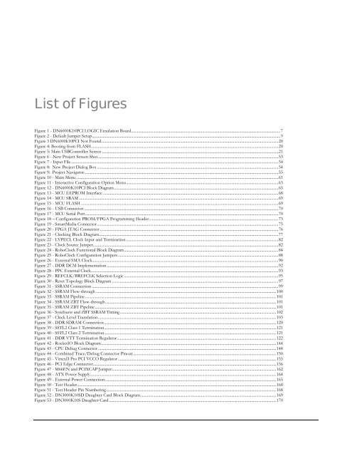
List of Figures<br />
Figure 1 - DN6000K10PCI LOGIC Emulation Board.....................................................................................................................................................7<br />
Figure 2 - Default Jumper Setup............................................................................................................................................................................................9<br />
Figure 3 DN6000k10PCI Not Found.................................................................................................................................................................................20<br />
Figure 4: Booting from FLASH...........................................................................................................................................................................................20<br />
Figure 5: Main USBController Screen ................................................................................................................................................................................21<br />
Figure 6 - New Project Screen Shot....................................................................................................................................................................................53<br />
Figure 7 - Input File...............................................................................................................................................................................................................54<br />
Figure 8: New Project Dialog Box .....................................................................................................................................................................................54<br />
Figure 9: Project Navigator..................................................................................................................................................................................................55<br />
Figure 10 - Main Menu..........................................................................................................................................................................................................61<br />
Figure 11 - Interactive Configuration Option Menu........................................................................................................................................................63<br />
Figure 12 - DN6000K10PCI Block Diagram....................................................................................................................................................................65<br />
Figure 13 - MCU EEPROM Interface ...............................................................................................................................................................................68<br />
Figure 14 - MCU SRAM .......................................................................................................................................................................................................69<br />
Figure 15 - MCU FLASH .....................................................................................................................................................................................................69<br />
Figure 16 - USB Connector ..................................................................................................................................................................................................70<br />
Figure 17 - MCU Serial Port.................................................................................................................................................................................................70<br />
Figure 18 – Configuration PROM/FPGA Programming Header.................................................................................................................................73<br />
Figure 19 - SmartMedia Connector.....................................................................................................................................................................................75<br />
Figure 20 - FPGA JTAG Connector ..................................................................................................................................................................................76<br />
Figure 21 - Clocking Block Diagram...................................................................................................................................................................................77<br />
Figure 22 - LVPECL Clock Input and Termination ........................................................................................................................................................82<br />
Figure 23 - Clock Source Jumper.........................................................................................................................................................................................82<br />
Figure 24 - RoboClock Functional Block Diagram..........................................................................................................................................................84<br />
Figure 25 - RoboClock Configuration Jumpers ................................................................................................................................................................88<br />
Figure 26 - External SMA Clock..........................................................................................................................................................................................90<br />
Figure 27 - DDR DCM Implementation ...........................................................................................................................................................................92<br />
Figure 28 - PPC External Clock...........................................................................................................................................................................................93<br />
Figure 29 - REFCLK/BREFCLK Selection Logic ..........................................................................................................................................................95<br />
Figure 30 - Reset Topology Block Diagram ......................................................................................................................................................................97<br />
Figure 31 - SSRAM Connection ..........................................................................................................................................................................................99<br />
Figure 32 - SSRAM Flow-through ....................................................................................................................................................................................100<br />
Figure 33 - SSRAM Pipeline...............................................................................................................................................................................................101<br />
Figure 34 - SSRAM ZBT Flow-through...........................................................................................................................................................................101<br />
Figure 35 - SSRAM ZBT Pipeline .....................................................................................................................................................................................101<br />
Figure 36 - Syncburst and ZBT SSRAM Timing ............................................................................................................................................................102<br />
Figure 37 - Clock Level Translation..................................................................................................................................................................................103<br />
Figure 38 - DDR SDRAM Connection............................................................................................................................................................................120<br />
Figure 39 - SSTL2 Class 1 Termination............................................................................................................................................................................121<br />
Figure 40 - SSTL2 Class 2 Termination............................................................................................................................................................................121<br />
Figure 41 - DDR VTT Termination Regulator...............................................................................................................................................................122<br />
Figure 42 - RocketIO Block Diagram...............................................................................................................................................................................144<br />
Figure 43 - CPU Debug Connector ..................................................................................................................................................................................148<br />
Figure 44 - Combined Trace/Debug Connector Pinout...............................................................................................................................................150<br />
Figure 45 - VirtexII Pro PCI VCCO Regulator ..............................................................................................................................................................155<br />
Figure 46 - PCI Edge Connector.......................................................................................................................................................................................156<br />
Figure 47 - M66EN and PCIXCAP Jumper....................................................................................................................................................................162<br />
Figure 48 - ATX Power Supply..........................................................................................................................................................................................164<br />
Figure 49 - External Power Connection...........................................................................................................................................................................165<br />
Figure 50 - Test Header.......................................................................................................................................................................................................168<br />
Figure 51 - Test Header Pin Numbering..........................................................................................................................................................................168<br />
Figure 52 - DN3000K10SD Daughter Card Block Diagram........................................................................................................................................169<br />
Figure 53 - DN3000K10S Daughter Card .......................................................................................................................................................................170
![SODIMM Schematic [PDF]](https://img.yumpu.com/43758171/1/190x146/sodimm-schematic-pdf.jpg?quality=85)
![User's Manual [PDF - 8.3MB]](https://img.yumpu.com/36435641/1/190x245/users-manual-pdf-83mb.jpg?quality=85)