Hardware Interface Description - Wireless Data Modules
Hardware Interface Description - Wireless Data Modules
Hardware Interface Description - Wireless Data Modules

Create successful ePaper yourself
Turn your PDF publications into a flip-book with our unique Google optimized e-Paper software.
MC55/56 <strong>Hardware</strong> <strong>Interface</strong> <strong>Description</strong><br />
Confidential / Released<br />
s<br />
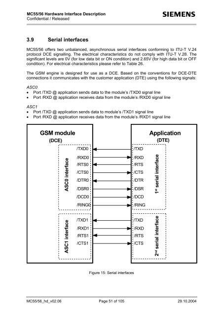
3.9 Serial interfaces<br />
MC55/56 offers two unbalanced, asynchronous serial interfaces conforming to ITU-T V.24<br />
protocol DCE signalling. The electrical characteristics do not comply with ITU-T V.28. The<br />
significant levels are 0V (for low data bit or ON condition) and 2.65V (for high data bit or OFF<br />
condition). For electrical characteristics please refer to Table 26.<br />
The GSM engine is designed for use as a DCE. Based on the conventions for DCE-DTE<br />
connections it communicates with the customer application (DTE) using the following signals:<br />
ASC0<br />
• Port /TXD @ application sends data to the module’s /TXD0 signal line<br />
• Port /RXD @ application receives data from the module’s /RXD0 signal line<br />
ASC1<br />
• Port /TXD @ application sends data to module’s /TXD1 signal line<br />
• Port /RXD @ application receives data from the module’s /RXD1 signal line<br />
GSM module<br />
(DCE)<br />
/TXD0<br />
/TXD<br />
Application<br />
(DTE)<br />
ASC0 interface<br />
/RXD0<br />
/RTS0<br />
/CTS0<br />
/DTR0<br />
/DSR0<br />
/DCD0<br />
/RXD<br />
/RTS<br />
/CTS<br />
/DTR<br />
/DSR<br />
/DCD<br />
1 st serial interface<br />
/RING0<br />
/RING<br />
ASC1 interface<br />
/TXD1<br />
/RXD1<br />
/RTS1<br />
/CTS1<br />
/TXD<br />
/RXD<br />
/RTS<br />
/CTS<br />
2 nd serial interface<br />
Figure 15: Serial interfaces<br />
MC55/56_hd_v02.06 Page 51 of 105 29.10.2004