Hardware Interface Description - Wireless Data Modules
Hardware Interface Description - Wireless Data Modules
Hardware Interface Description - Wireless Data Modules

You also want an ePaper? Increase the reach of your titles
YUMPU automatically turns print PDFs into web optimized ePapers that Google loves.
MC55/56 <strong>Hardware</strong> <strong>Interface</strong> <strong>Description</strong><br />
Confidential / Released<br />
s<br />
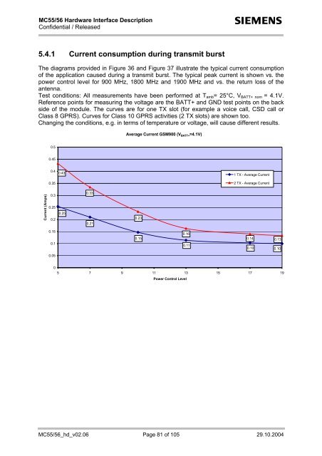
5.4.1 Current consumption during transmit burst<br />
The diagrams provided in Figure 36 and Figure 37 illustrate the typical current consumption<br />
of the application caused during a transmit burst. The typical peak current is shown vs. the<br />
power control level for 900 MHz, 1800 MHz and 1900 MHz and vs. the return loss of the<br />
antenna.<br />
Test conditions: All measurements have been performed at T amb = 25°C, V BATT+ nom = 4.1V.<br />
Reference points for measuring the voltage are the BATT+ and GND test points on the back<br />
side of the module. The curves are for one TX slot (for example a voice call, CSD call or<br />
Class 8 GPRS). Curves for Class 10 GPRS activities (2 TX slots) are shown too.<br />
Changing the conditions, e.g. in terms of temperature or voltage, will cause different results.<br />
Average Current GSM900 (V BATT+ =4.1V)<br />
0.5<br />
0.45<br />
0.4<br />
0.35<br />
0.43<br />
1 TX - Average Current<br />
2 TX - Average Current<br />
Current (Amps)<br />
0.3<br />
0.25<br />
0.2<br />
0.25<br />
0.33<br />
0.21<br />
0.23<br />
0.15<br />
0.1<br />
0.15<br />
0.16<br />
0.11<br />
0.14<br />
0.10<br />
0.13<br />
0.10<br />
0.05<br />
0<br />
5 7 9 11 13 15 17 19<br />
Power Control Level<br />
MC55/56_hd_v02.06 Page 81 of 105 29.10.2004