V. Focused Fundamental Research - EERE - U.S. Department of ...
V. Focused Fundamental Research - EERE - U.S. Department of ...
V. Focused Fundamental Research - EERE - U.S. Department of ...

Create successful ePaper yourself
Turn your PDF publications into a flip-book with our unique Google optimized e-Paper software.
Vaughey – ANL<br />
V.C.7 Three-Dimensional Anode Architectures and Materials (ANL)<br />
Approach<br />
· Design new electrode architectures by<br />
electrodeposition techniques in which a Cu foam<br />
provides an electronically connected substrate onto<br />
which electrochemically active metals can be<br />
deposited.<br />
· Develop methods to build electrodes where copper<br />
metal acts as a binder and conductive additive for high<br />
capacity main group metals, e.g. silicon.<br />
· Develop characterization methods that allow for a<br />
better understanding <strong>of</strong> the electrochemically active<br />
interfaces with in the electrode architecture.<br />
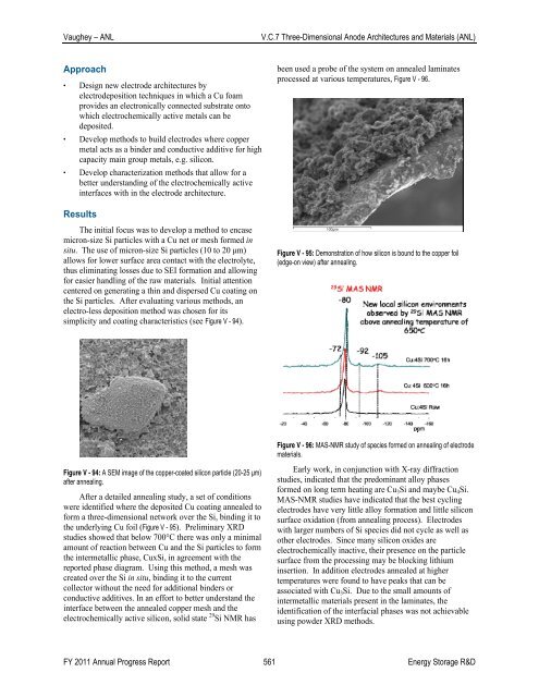
been used a probe <strong>of</strong> the system on annealed laminates<br />
processed at various temperatures, Figure V - 96.<br />
Results<br />
The initial focus was to develop a method to encase<br />
micron-size Si particles with a Cu net or mesh formed in<br />
situ. The use <strong>of</strong> micron-size Si particles (10 to 20 μm)<br />
allows for lower surface area contact with the electrolyte,<br />
thus eliminating losses due to SEI formation and allowing<br />
for easier handling <strong>of</strong> the raw materials. Initial attention<br />
centered on generating a thin and dispersed Cu coating on<br />
the Si particles. After evaluating various methods, an<br />
electro-less deposition method was chosen for its<br />
simplicity and coating characteristics (see Figure V - 94).<br />
Figure V - 95: Demonstration <strong>of</strong> how silicon is bound to the copper foil<br />
(edge-on view) after annealing.<br />
Figure V - 96: MAS-NMR study <strong>of</strong> species formed on annealing <strong>of</strong> electrode<br />
materials.<br />
Figure V - 94: A SEM image <strong>of</strong> the copper-coated silicon particle (20-25 μm)<br />
after annealing.<br />
After a detailed annealing study, a set <strong>of</strong> conditions<br />
were identified where the deposited Cu coating annealed to<br />
form a three-dimensional network over the Si, binding it to<br />
the underlying Cu foil (Figure V - 95). Preliminary XRD<br />
studies showed that below 700°C there was only a minimal<br />
amount <strong>of</strong> reaction between Cu and the Si particles to form<br />
the intermetallic phase, CuxSi, in agreement with the<br />
reported phase diagram. Using this method, a mesh was<br />
created over the Si in situ, binding it to the current<br />
collector without the need for additional binders or<br />
conductive additives. In an effort to better understand the<br />
interface between the annealed copper mesh and the<br />
electrochemically active silicon, solid state 29 Si NMR has<br />
Early work, in conjunction with X-ray diffraction<br />
studies, indicated that the predominant alloy phases<br />
formed on long term heating are Cu 3 Si and maybe Cu 4 Si.<br />
MAS-NMR studies have indicated that the best cycling<br />
electrodes have very little alloy formation and little silicon<br />
surface oxidation (from annealing process). Electrodes<br />
with larger numbers <strong>of</strong> Si species did not cycle as well as<br />
other electrodes. Since many silicon oxides are<br />
electrochemically inactive, their presence on the particle<br />
surface from the processing may be blocking lithium<br />
insertion. In addition electrodes annealed at higher<br />
temperatures were found to have peaks that can be<br />
associated with Cu 3 Si. Due to the small amounts <strong>of</strong><br />
intermetallic materials present in the laminates, the<br />
identification <strong>of</strong> the interfacial phases was not achievable<br />
using powder XRD methods.<br />
FY 2011 Annual Progress Report 561 Energy Storage R&D