

mitsubishi - Al Kossow's Bitsavers
mitsubishi - Al Kossow's Bitsavers
mitsubishi - Al Kossow's Bitsavers

You also want an ePaper? Increase the reach of your titles
YUMPU automatically turns print PDFs into web optimized ePapers that Google loves.
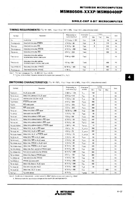
MITSUBISHI MICROCOMPUTERSMSM80S0H-XXXP IMSM8040HPSINGLE-CHIP a-BIT MICROCOMPUTERTIMING REQUIREMENTS (Ta=0-70"C, Vcc=Voo=5V± 10%, VSS =0 V, unless otherwise noted)UnitSymbolParameterRelationship to <strong>Al</strong>ternativeLimitscycle time (to) symbol Min Typ MaxtW(To) TO pulse period 3/15·tet OPRR 270 nste Cycle time l/(fxTAL -;-.15) tCY 1. 36 15 liSt h(PSEN-O) Data hold time after P SEN 1/10·te -30 tOR 0 110 nsth(R-O) Data hold time after R D 1/10,te-30 tOR 0 110 nstSU(PSEN-O) Data setup time after P SEN 3/10·te-200 tR02 210 nstSU(R-O) Data setup time after R D 2/5·te-200 tROI 350 nstsul (A-O)Data setup time after address(external data memory read cycle)7/10-te-22OtAOInstSU2(A-O)Data setup time after address(external program memory read cycle) 1/2·te-2OO tA02 460 nstsu (PROG-O) Data setup time after PROG 6/10·te-120 tpR 700 nsth (PROG-O) Data hold time after PROG 1/10-te tpF 0 140 nsNote 1: The input voltages are V IL = 0,45 V and V I H = 2 , 4 V.2: f ~TAL is the oscillator frequency entered at the crystal input terminals (X I , X 2 ).SymbolParameterRelationship to <strong>Al</strong>ternativeLimitscycle time (te) symbol Min Typ MaxUnittW(ALE) ALE pulse width 7/30-te-170 t LL 150nstd (A-ALE) Delay time, address to ALE signal 2/15- te-110 tAL 70nstv (ALE-A) Address valid time after ALE 1/ 15·te -40t LA 50nstW(PSEN) P SEN pulse width 2/5·te-200tCC2 350nstW(R) RD pulse width 1/2·te-200 tCCI 480nstw(W) WR pulse width 1/2·te-200 tCCI 480nstd (Q-W) Delay time, data to W R signal 13/30' te - 200 tow 390nstv (W-Q) Data valid time after WR 1/15·te-50 two 40nstd (A-W) Delay time, address to W R signal 1/3-tc-15O tAW 300nstd (AZ-R) Delay time, address disable to R D signal 2/ 15-te -40t AFCI 140nstd (AZ-W) Delay time, address disable to WR signal 2/15-te-40t AFCI .,40nstd (AZ-PSEN) Delay time, address disable to P SEN signal 1/30·te-40t AFC2 10nstd (ALE-R) Delay time, ALE to RD signal 1/5·te-75t LAFCI 200nstd (ALE-W) Delay time, ALE to W R signal 1/5·te-75t LAFCI 200nstd (ALE-PSEN) Delay time, ALE to PSEN signal 1/10·te-75t LAFC2 60nstd (R-ALE) Delay time, RD to ALE signal 1/15·te -40 tCAI 50nstd (W-ALE) Delay time, WR to ALE signal 1/15·te-40 tCAI 50nstd (PROG-ALE). Delay time, PROG to ALE signal 1/15·te-40 tCAI 50nstd (PSEN-ALE) Delay time, PSEN to ALE signal 4/15-tc-40tCA2 320nstd (PC-PROG) Delay time, Port control to PROG signal 2/15- t c-;-80 tcp 100nstv (PROG-PC) Port control valid time after PROG 4/15·te-200 t pc 160nstd (Q-PROG) Delay time, Data to PROG signal 2/5·te-150 top 400nstv (PROG-Q) Data valid time after PROG 1/10·te-50t po 90nstW(PROGL) PROG low pulse width 7/10·te-250 tpp 700nstd (Q-ALE) Delay time, Daia to ALE signal 4/15·te-200 t pL 160nstv (ALE-Q) Data valid time after ALE 1/10·te-l00 t LP 40nstd (ALE-Q) Delay time, A LE to data 3/10·te + 100 t pv 510 nsSWITCHING CHARACTERISTICS (Ta=0-70"C, V cc =V 00 =5V ± 10%. V SS =OV, unlessotlierwise noted)aNote 3: Conditions of measurement: control output CL =8OpF data bus output, port output C L=150pF.4: Reference levels for input/output voltages are low-level=0.8V and high-level=2V.• MITSUBISHI.... ELECTRIC4-37


