

mitsubishi - Al Kossow's Bitsavers
mitsubishi - Al Kossow's Bitsavers
mitsubishi - Al Kossow's Bitsavers

Create successful ePaper yourself
Turn your PDF publications into a flip-book with our unique Google optimized e-Paper software.
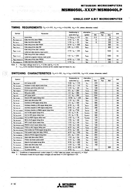
MITSUBISHI MICROCOMPUTERSMSM80S0L.XXXP/MSM8040LPSINGLE-CHIP I-BIT MICROCOMPUTERTIMING REQUIREMENTS (Ta = 0:....70·C. Vee = Voo = 5V±10%, Vss = ov. unless otherwise noted)SymbolParameterRelationship to <strong>Al</strong>ternative Limitseycle time (t c ) symbol Min Typtc Cycle time 11 (fxTAL -+- 15) tCY 2.5th (PSEN-O) Data hold time after PSEN 1/10· tc - 30 tOR 0th (R-O) Data hold time after RD 1/10· tc - 30 tOR 0tsu (PSEN-O) Data setup time after PSEN 3/10· tc - 200 tR02tsu (R-O) Data setl,lp t!m,e after RD 2/5' tc - 200 tR01tSUl (A-D)Data setup time after address(external data memory read cycle)7/10· tc - 220 tAOltSU2 (A-D)Data setup time after address(external program memory read cycle)1/2·tc -200tsu (PROG-O) Data setup time after PROG 6/10· tc - 120 tpRth (PROG-O) Data hold time after PROG 1/10· tc tpF 0NoteThe input voltage level is V1L = O. 45V and V1H = 2.4V.fXTAL is the oscillator frequency entered at the crystal input terminals (Xl. X 2 ).tA02UnitMax15 J,lS220 ns220 ns550 ns800 ns1530 ns1050 ns1380 ns250 nsSWITCHING CHARACTERISTICS (Ta = 0-7ot. Vee = Voo = 5V±10%, Vss = ov. unless otherwise noted)SymbolParameterRelationship tocycle time (tel<strong>Al</strong>ternativetw (ALE) ALE pulse width 7/3Q • tc - 170 tLLtd (A-ALE) Address to ALE signal delay time 2115 • tc - 110 tALtv (ALE-A) Address vaUd time after ALE 1/15· tc - 40 tLAsymboltw (PSEN) PSEN pulse width 2/5, tc - 200 tcc2tw (R) RD pulse width 1/2·tc -200 tCCltw(W) WR pulse width 1/2·tc -200 tCCltd (O-W) Data to WR signal delay time 13/30, tc - 200 towtv (w-o) Data vaUd time after WR 1/15· tc - 50 twotd (A-W) Address to WR, signal delay time 1/3·tc -150 tAWtd (AZ-R) Address disable to RD signal delay time 2/15· tc - 40 tAFCltd (AZ-W) Address disable to WR signal delay time 2/15· tc - 40 tAFCltd (AZ-PSEN) Address disable to PSEN signal delay time 1/30· tc ~·40 tAFC2td (ALE-R) ALE to RD signal delay time 1/5·tc -75 tLAFCltd (ALE-W) ALE to WR signal delay time 1/5' tc -75 t LAFCltd (ALE-PSEN) ALE to PSEN Signal delay time 1/10·tc -75 tLAFC2td (R-ALE) RD to ALE signal delay time 1/15·tc -40 tC<strong>Al</strong>td (W-ALE) WR to ALE signal delay time 1/15· tc - 40 tC<strong>Al</strong>td (PROG-ALE) PROG to ALE Signal delay time 1/15·tc -40 tC<strong>Al</strong>td (PSEN-ALE) PSEN to ALE signal delay time 4/15· tc - 40 tCA2td (PC-PROG) Port control to PROG signal delay time 2/15· tc - 80 tcptv (PROG-PC) Port control valid time after PROG 4/15· tc - 200 tpctd (O-PROG) Data to PROG signal delay time 2/5· tc -150 toptv (PROG-O) Data vaUd time after PROG 1/10·tc -50 tpotw (PROGLl PROG low-level pulse width 7/10· tc - 250 tpptd (a-ALE) Data to ALE signal delay time 4/15· tc - 200 tpLtv (ALE-a) Data valid time after ALE 1/10· tc -100 t LPtd (ALE-a) Delay time after ALE 3/10· tc + 100 tpvtw ("0) To pulse spacing 3/15· tc toPRRNote 34Conditions of measurement: control output CL = 80pF data bus output. port output CL = 150pF.Reference levels for input/output voltages are low-level = 0.8V high-level = 2V .Min41022012080010501050880120680290290404204201701201201206202504608502001500460150500LimitsTypUnitMaxnsnsnsnsnsnsnsnsnsnsnsnsnsnsnsnsnsnsnsnsnsnsnsnsnsns850 nsns4-42 . •.. MITSUBISHI.... ELECTRIC


