

mitsubishi - Al Kossow's Bitsavers
mitsubishi - Al Kossow's Bitsavers
mitsubishi - Al Kossow's Bitsavers

Create successful ePaper yourself
Turn your PDF publications into a flip-book with our unique Google optimized e-Paper software.
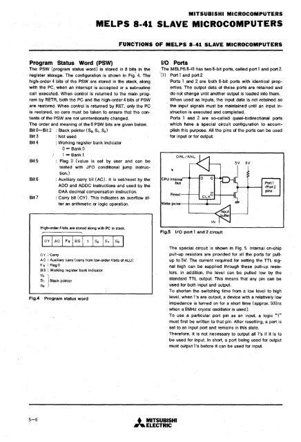
MITSUBISHI MICROCOMPUTERSMELPS 8-41 SLAVEM-ICROCOMPUTERSFUNCTIONS OF MELPS 8-41 SLAVE MICROCOMPUTERSProgram Status Word (PSW)The PSW (program status word) is stored in 8 bit~ in theregister storage. The configuration is shown in Fig. 4. Thehigh-order 4 bits of the PSW are stored in the stack, alongwith the PC, when an interrupt is accepted or a subroutin~call executed. When control is returned to the main programby RETR, both the PC and the high-order 4 bits of PSWare restored. When control is returned by RET, only the PCis restored, so care must be taken to ensure that the contentsof the PSW are not unintentionally changed.The order and meaning of the 8 PSW bits are given below.Bit O-Bit 2 : Stack pointer (So, S1, S2)Bit 3 : Not usedBit 4 : Working register bank indicator0= BankO1 = Bank 1Bit 5 Flag 0 (value is set by user and can betested with JFO conditional jump instruction.)Bit6 : Auxiliary carry bit (AC). It is set/reset by theADD and ADDC instructions and used by theDAA decimal compensation instruction.Bit7 : Carry bit (CY). This indicates an overflow afteran arithmetic or logic operation.1/0 PortsThe MELPS 8-41 has two 8-bit ports, called port 1 and port 2.'(1) Port 1 and port 2Ports 1 and 2 are both 8-bit ports with identical properties.The output data of these ports are retained anddo not change until another output is loaded into them.. When used as inputs, the input data is not retained. sothe input signals must be maintained until an input instructionis executed and completed ..Ports 1 and 2 are so-called quasi-bidirectional portswhich have a special circuit configuration to accomplishthis purpose. <strong>Al</strong>l the pins of the ports can be usedfor input or for output.CPU interna~""'--IbusReset -+---1Write pulse--+----+------l5VPortl~~~--t IPort 2pinsFlg.4High-order 4 bits are stored along with PC in stack.I Cy I AC I Fo I as 11 I S2 I S1 I So ICy : CarryA C : Auxiliary carry '( carry from low-order 4 bits of ALU)Fo : Flag 0as : Working register bank indicatorS2 }S 1 Stack pointerSoProgram status wordFlg.51/0 port 1 and 2 circuitThe special, circuit is shown in Fig. 5. Internal on-chippull-up resistors are provided for all the ports for pullupto 5V. The current required for setting the TTL signalhigh can be supplie(J through these pull-up resistors.In addition, the level can be pulled low by thestandard TTL output. This means that any pin can beused for both input and output.To shorten the switching time from a low level to highlevel, when l's are output, a device with a relatively lowimpedance is turned on for a short time (approx. 500nswhen a 6MHz crystal oscillator is used).To use a particular port pin as an input, a logic "1"must first be written to that pin. After resetting, a port isset to an input port and remains in this state.Therefore, it is not necessary to output all l's if it is tobe used for input. In short, a port being used for outputmust output l's before it can be used for input.5-6 • MITSUBISHI..... ELECTRIC


