

mitsubishi - Al Kossow's Bitsavers
mitsubishi - Al Kossow's Bitsavers
mitsubishi - Al Kossow's Bitsavers

You also want an ePaper? Increase the reach of your titles
YUMPU automatically turns print PDFs into web optimized ePapers that Google loves.
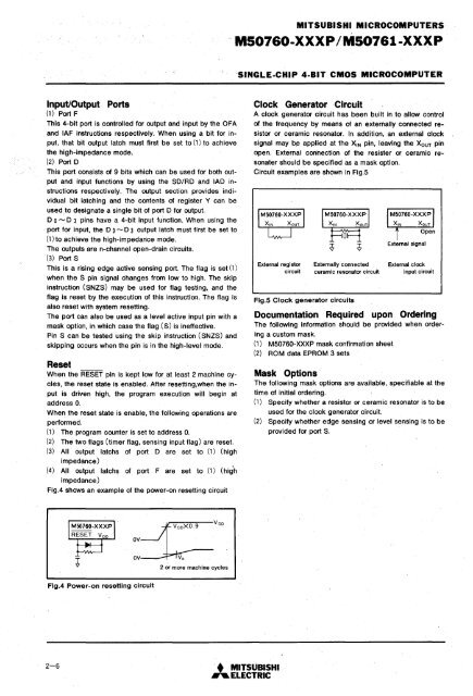
MITSUBISHI MICROCOMPUTERSMS0760-XXXP IMS0761-XXXP'SINGLE-CHIP 4-BIT CMOS MICROCOMPUTERInput/Output Ports(1) Port FThis 4-bit port is controlled for output and input by the OFAand IAF instructions respectively. When using a bit for input,that bit output latch must first be set to (1) to achievethe high-impedance mode.(2) Port 0This port consists of 9 bits which can be used for both outputand input functions by using the SO/RO and lAD instructionsrespectively. The output section provides individualbit latching and the contents of register Y can beusedto designate a single bit of port 0 for output.o 0 ...., 0 3 pins have a 4-bit input function. When using theport for input, the DO ....... 03 output latch must first be set to(1) to achieve the high-impedance mode.The outputs are n-channel open-drain circuits.(3) Port SThis is a rising edge active sensing port. The flag is set (1)when the S pin signal changes from low to high. The skipinstruction (SNZS) may be used for flag testing, and theflag is reset by the execution of this instruction. The flag isalso reset with system resetting.The port can also be used as a level active input pin with amask option, in which case the flag (S) is ineffective.Pin S can be tested using the skip instruction (SNZS) andskipping occurs when the pin is in the high-level mode.ResetWhen the RESET pin is kept low for at least 2 machine cycles,the reset state is enabled. After resetting,when the inputis driven high, the program execution will begin ataddress O.When the reset state is enable, the following operations areperformed.(1) The program counter is set to address O.(2) The two flags (timer flag, sensing input flag) are reset.(3) <strong>Al</strong>l output latchs of port 0 are set to (1) (highimpedance)(4) <strong>Al</strong>l output latchs of port F are set to (1) (hig'himpedance)Fig.4 shows an' example of the power-on resetting circuitClock Generator CircuitA clock generator circuit has been built in to allow controlof the frequency by means of an externally connected resistoror ceramic resonator. In addition, an external clockSignal may be applied at the X 1N pin, leaving the X OUT pinopen. External con'nection of the resister or ceramic resonatershould be specified as a mask option.Circuit examples are shown in Fig.5External registorcircuitExternally connectedceramic resonator circuitFlg.5 Clo,ck generator circuitsExternal signalExternal clockinput circuitDocumentation Required upon OrderingThe following information should be provided when orderinga custom mask.(1) M50760-XXXP mask confirmation sheet(2) ROM data EPROM 3 setsMask OptionsThe following mask options are available, specifiable at thetime of initial ordering.(1) Specify whether a resistor or ceramic resonator is to beused for the clock generator circuit.(2) Specify whether edge sensing or level sensing is to beprovided for port S.Flg.4 Power-on resetting circuitOV~.VDDOV~2 or more machine cycles2-6'. MITSUBISHI.... ELECTRIC


