

Hacking_and_Penetration_Testing_with_Low_Power_Devices

Create successful ePaper yourself
Turn your PDF publications into a flip-book with our unique Google optimized e-Paper software.
132 CHAPTER 6 Input <strong>and</strong> output devices<br />
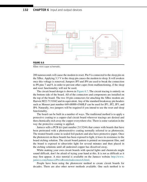
FIGURE 6.6<br />
XBee mini-cape schematic.<br />
200 nanoseconds will cause the modem to reset. Pin 9 is connected to the sleep pin on<br />
the XBee. Applying 3.3 V to the sleep pin causes the modem to sleep. It will awaken<br />
once this voltage is removed. Jumpers JP3 <strong>and</strong> JP4 are used to break the connection<br />
to P8 pins 7 <strong>and</strong> 9, in order to prevent other capes from malfunctioning, if the sleep<br />
<strong>and</strong> reset functionality will not be used.<br />
The circuit board design is shown in Figure 6.7. The circuit tracing is entirely on<br />
the bottom side of the board. All of the connectors <strong>and</strong> components are installed on<br />
the top of the board. The two 10-pin connectors for attaching the XBee modem are<br />
Harwin M22-7131042 <strong>and</strong> its equivalent. Any of the st<strong>and</strong>ard breakaway pin headers<br />
such as Mouser part number 649-68000-436HLF can be used for JP1, JP2, JP3, <strong>and</strong><br />
JP4. Naturally, two jumpers will be required if you intend to use the reset <strong>and</strong> sleep<br />
functionality.<br />
The board can be built in a number of ways. The traditional method is to apply a<br />
protective coating to a copper-clad circuit board wherever tracings are desired <strong>and</strong><br />
then chemically etch away the copper everywhere else. There is some variation in the<br />
way the protective coating is applied.<br />
Jameco sells a PCB kit (part number 2113244) that comes <strong>with</strong> boards that have<br />
been pretreated <strong>with</strong> a photosensitive coating normally referred to as photoresist.<br />
The treated boards come in sealed foil packets <strong>and</strong> also have protective paper. Once<br />
the photoresist on these boards has been exposed to light, it loses its resistance to the<br />
board etching solution. The circuit board pattern is printed on transparent film, <strong>and</strong><br />
the board is exposed to ultraviolet light for several minutes <strong>and</strong> then placed in<br />
the etching solutions until all undesired copper has dissolved away.<br />
While making your own circuit boards <strong>with</strong> special lights <strong>and</strong> chemicals might<br />
sound difficult, don’t be afraid of trying your h<strong>and</strong> at this. It is not as difficult as it<br />
may first appear. A nice tutorial is available on the Jameco website http://www.<br />
jameco.com/Jameco/PressRoom/makeoneetch.html.<br />
People have been using the photoresist method to create circuit boards for<br />
decades. There are also other newer methods available. One such method is to