

Application Note AN-1150 - International Rectifier
Application Note AN-1150 - International Rectifier
Application Note AN-1150 - International Rectifier

You also want an ePaper? Increase the reach of your titles
YUMPU automatically turns print PDFs into web optimized ePapers that Google loves.
3.3.3 Dedicated Overvoltage Protection Divider (OVP/EN pin)<br />
In addition to the overvoltage comparator on VFB pin, IR1152 features a 2nd<br />
overvoltage comparator (designated the OVP(OVP) in the IC block diagram)<br />
which is connected to the OVP/EN pin. The OVP(OVP) comparator is identical in<br />
design to the OVP(VFB) comparator and also references the same trigger and<br />
re-enable thresholds of 106% and 103% of V REF respectively. The VFB pin<br />
resistor divider calculated earlier is applicable for the OVP/EN pin also. Hence,<br />
for this converter, 1Mohm, 1% tolerance resistor is selected for R OVP1 & R OVP2<br />
and 26.1kΩ, 1% tolerance resistor is selected for R OVP3 . The trigger and reenable<br />
set-points calculated earlier are likewise applicable here too.<br />
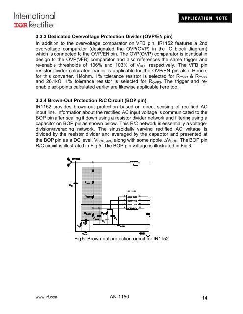
3.3.4 Brown-Out Protection R/C Circuit (BOP pin)<br />
IR1152 provides brown-out protection based on direct sensing of rectified AC<br />
input line. Information about the rectified AC input voltage is communicated to the<br />
BOP pin after scaling it down using a resistor divider network and filtering using a<br />
capacitor on BOP pin as shown below. This R/C network is essentially a voltagedivision/averaging<br />
network. The sinusoidally varying rectified AC voltage is<br />
divided by the resistor divider and averaged by the capacitor and presented at<br />
the BOP pin as a DC level, V BOP, AVG along with some ripple, ∆V BOP . The BOP pin<br />
R/C circuit is illustrated in Fig.5. The BOP pin voltage is illustrated in Fig.6.<br />
Bridge<br />
+<br />
L BST<br />
R BOP1<br />
C IN<br />
R BOP2<br />
R BOP3<br />
IR1152<br />
IR1145<br />
C BOP R gm 1<br />
COM<br />
GATE 8<br />
2<br />
COMP<br />
VCC 7<br />
3<br />
ISNS<br />
VFB 6<br />
4<br />
BOP<br />
OVP/EN 5<br />
C P<br />
C<br />
R SF<br />
C SF<br />
C Z<br />
COM<br />
R SNS<br />
GND<br />
Fig 5: Brown-out protection circuit for IR1152<br />
www.irf.com <strong>AN</strong>-<strong>1150</strong><br />
14


