

Application Note AN-1150 - International Rectifier
Application Note AN-1150 - International Rectifier
Application Note AN-1150 - International Rectifier

You also want an ePaper? Increase the reach of your titles
YUMPU automatically turns print PDFs into web optimized ePapers that Google loves.
Output voltage sensor Resistor-Divider, H 1 (s)<br />
The output divider scales the output voltage to be compared with the reference<br />
voltage in the error amplifier.<br />
Therefore:<br />
V<br />
OUT<br />
( R<br />
=<br />
FB1 + RFB2<br />
+ RFB3)<br />
VREF<br />
R<br />
V<br />
H<br />
1<br />
( s)<br />
=<br />
V<br />
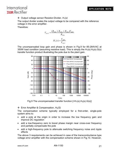
The uncompensated loop gain and phase is shown in Fig.9 for 85-264VAC at<br />
350W load condition (assuming resistive load). This is simply the H 1 (s).H 3 (s).G(s)<br />
transfer function product illustrating the pole due to the plant gain.<br />
FB3<br />
REF<br />
OUT<br />
90<br />
60<br />
30<br />
0<br />
Gain 85VAC Uncompensated<br />
Gain 264VAC Uncompensated<br />
Phase 85VAC Uncompensated<br />
Phase 264VAC Uncompensated<br />
90<br />
60<br />
30<br />
0<br />
Gain (dB)<br />
-30<br />
-60<br />
-90<br />
-120<br />
-150<br />
-30<br />
-60<br />
-90<br />
-120<br />
-150<br />
Phase (deg)<br />
-180<br />
-180<br />
0.01 0.1 1 10 100 1000 10000 100000<br />
f (Hz)<br />
Fig.9 The uncompensated transfer function [=H 1 (s).H 3 (s).G(s)]<br />
Error Amplifier & Compensation, H 2 (S)<br />
The compensation scheme typically employed for a first-order, single-pole<br />
system aims to:<br />
• add a pole at the origin in order to increase the low frequency gain and<br />
improve DC regulation<br />
• add a low-frequency zero to boost phase margin near cross-over frequency<br />
and partially compensate the pole<br />
• add a high-frequency pole to attenuate switching frequency noise and ripple<br />
effects<br />
The above 3 requirements can be achieved in case of the transconductance type<br />
voltage error amplifier with the compensation scheme shown in Fig.10. However,<br />
www.irf.com <strong>AN</strong>-<strong>1150</strong><br />
21


