

Application Note AN-1150 - International Rectifier
Application Note AN-1150 - International Rectifier
Application Note AN-1150 - International Rectifier

You also want an ePaper? Increase the reach of your titles
YUMPU automatically turns print PDFs into web optimized ePapers that Google loves.
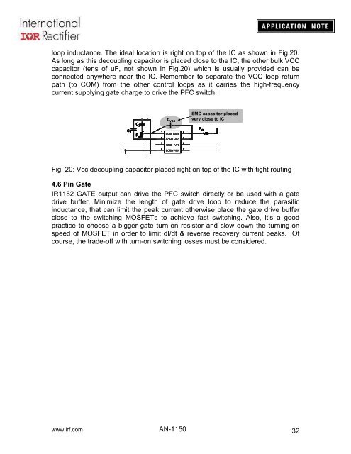
loop inductance. The ideal location is right on top of the IC as shown in Fig.20.<br />
As long as this decoupling capacitor is placed close to the IC, the other bulk VCC<br />
capacitor (tens of uF, not shown in Fig.20) which is usually provided can be<br />
connected anywhere near the IC. Remember to separate the VCC loop return<br />
path (to COM) from the other control loops as it carries the high-frequency<br />
current supplying gate charge to drive the PFC switch.<br />
SMD capacitor placed<br />
C VCC very close to IC<br />
C Z<br />
R C G<br />
P 1<br />
COM<br />
GATE R 8<br />
gm 2<br />
COMP<br />
VCC 7<br />
3<br />
ISNS<br />
VFB 6<br />
4<br />
BOP<br />
OVP/EN 5<br />
Fig. 20: Vcc decoupling capacitor placed right on top of the IC with tight routing<br />
4.6 Pin Gate<br />
IR1152 GATE output can drive the PFC switch directly or be used with a gate<br />
drive buffer. Minimize the length of gate drive loop to reduce the parasitic<br />
inductance, that can limit the peak current otherwise place the gate drive buffer<br />
close to the switching MOSFETs to achieve fast switching. Also, it’s a good<br />
practice to choose a bigger gate turn-on resistor and slow down the turning-on<br />
speed of MOSFET in order to limit dI/dt & reverse recovery current peaks. Of<br />
course, the trade-off with turn-on switching losses must be considered.<br />
www.irf.com <strong>AN</strong>-<strong>1150</strong><br />
32


