

Application Note AN-1150 - International Rectifier
Application Note AN-1150 - International Rectifier
Application Note AN-1150 - International Rectifier

You also want an ePaper? Increase the reach of your titles
YUMPU automatically turns print PDFs into web optimized ePapers that Google loves.
1. Introduction<br />
The IR1152 IC is a fixed 66kHz frequency PFC IC designed to operate in<br />
continuous conduction mode Boost converters with average current mode<br />
control. The IC is packed with an impressive array of advanced features such as<br />
programmable soft-start, micro-power startup current, user initiated micro-power<br />
Sleep mode for compliance with stand-by energy standards, ultra low bias<br />
currents for sensing pins. The fixed internal oscillator ensures stable operation at<br />
66kHz switching frequency with very low gate jitter thus eliminating audible noise<br />
in PFC magnetics. In addition, the IC offers input-line sensed brown-out<br />
protection (BOP), “dual & dedicated” overvoltage protection, cycle-by-cycle peak<br />
current limit, open loop protection (OLP) and VCC under voltage lock-out<br />
(UVLO). All these features are offered in a compact 8-pin package making<br />
IR1152 the most feature-intensive IC for PFC applications. This application note<br />
provides an overview of IR1152 and demonstrates the design of a universal input<br />
350W AC-DC Boost PFC Converter. Design & layout tips are also included.<br />
2. IR1152 – Detailed Description<br />
2.1 Overview of IR1152<br />
AC Line<br />
Bridge<br />
- +<br />
AC Neutral<br />
L BST<br />
D BST<br />
V OUT<br />
C IN<br />
R gm C BOP C P<br />
C VCC<br />
R VFB3<br />
R BOP3<br />
R VFB1<br />
R BOP1<br />
IR1152<br />
IR1145<br />
R BOP2<br />
1<br />
COM<br />
GATE 8<br />
R G<br />
C OUT<br />
R VFB2<br />
2<br />
COMP<br />
VCC 7<br />
V CC<br />
M BST<br />
3<br />
ISNS<br />
VFB 6<br />
4<br />
BOP<br />
OVP/EN 5<br />
R OVP1<br />
R OVP2<br />
R OVP3<br />
R SF<br />
C SF<br />
C Z<br />
COM<br />
R SNS<br />
GND<br />
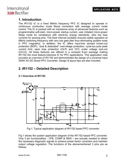
Fig.1: Typical application diagram of IR1152 based PFC converter<br />
Fig.1 shows the system application diagram of the IR1152 based PFC converter.<br />
Only 3 pin functionalities - VFB, COMP & ISNS – are actually needed to obtain<br />
the necessary diagnostic signals to achieve power factor correction and maintain<br />
output voltage regulation. The functions of the abovementioned 3 pins are as<br />
follows:<br />
www.irf.com <strong>AN</strong>-<strong>1150</strong><br />
2


