

Application Note AN-1150 - International Rectifier
Application Note AN-1150 - International Rectifier
Application Note AN-1150 - International Rectifier

Create successful ePaper yourself
Turn your PDF publications into a flip-book with our unique Google optimized e-Paper software.
900mV<br />
V BOP<br />
750mV<br />
∆V BOP<br />
V BOP,AVG<br />
SEL>><br />
600mV<br />
80V<br />
V(R2:2)<br />
V IN<br />
40V<br />
0V<br />
1/2f AC<br />
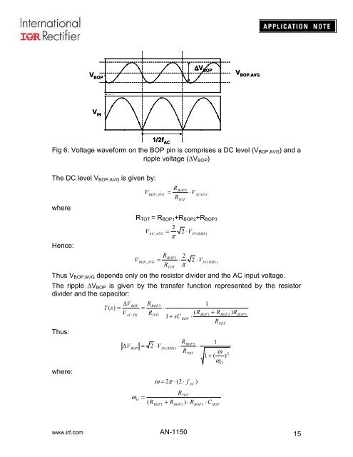
Fig 6: Voltage waveform on the BOP pin is comprises a DC level (V BOP,AVG ) and a<br />
ripple voltage (∆V BOP )<br />
The DC level V BOP,AVG is given by:<br />
where<br />
V<br />
BOP,<br />
AVG<br />
=<br />
R<br />
BOP3<br />
R<br />
TOT<br />
⋅V<br />
ACAVG<br />
Hence:<br />
R TOT = R BOP1 +R BOP2 +R BOP3<br />
2<br />
VAC, AVG<br />
= 2 ⋅VIN<br />
( RMS)<br />
π<br />
V<br />
R<br />
2<br />
BOP3<br />
BOP, AVG<br />
= ⋅ 2<br />
RTOT<br />
π<br />
⋅V<br />
IN ( RMS )<br />
Thus V BOP,AVG depends only on the resistor divider and the AC input voltage.<br />
The ripple ∆V BOP is given by the transfer function represented by the resistor<br />
divider and the capacitor:<br />
Thus:<br />
where:<br />
∆V<br />
T ( s)<br />
=<br />
V<br />
R<br />
=<br />
⋅<br />
BOP BOP3<br />
AC , PK<br />
R<br />
( R<br />
TOT<br />
BOP1<br />
+ RBOP<br />
2<br />
)<br />
1 + sC<br />
BOP<br />
⋅<br />
RTOT<br />
∆ V<br />
BOP<br />
=<br />
ω<br />
O<br />
=<br />
( R<br />
2 ⋅V<br />
IN ( RMS )<br />
R<br />
⋅<br />
R<br />
BOP3<br />
TOT<br />
ω = 2π<br />
⋅ (2 ⋅ f<br />
AC<br />
)<br />
R<br />
TOT<br />
BOP1 + RBOP<br />
2<br />
) ⋅<br />
R<br />
⋅<br />
BOP3<br />
1<br />
1<br />
ω<br />
1 + ( )<br />
ω<br />
⋅ C<br />
BOP<br />
O<br />
2<br />
R<br />
BOP3<br />
www.irf.com <strong>AN</strong>-<strong>1150</strong><br />
15


