

Application Note AN-1150 - International Rectifier
Application Note AN-1150 - International Rectifier
Application Note AN-1150 - International Rectifier

You also want an ePaper? Increase the reach of your titles
YUMPU automatically turns print PDFs into web optimized ePapers that Google loves.
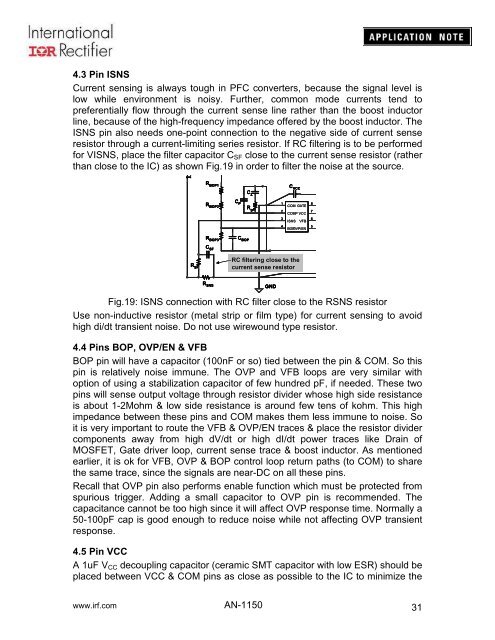
4.3 Pin ISNS<br />
Current sensing is always tough in PFC converters, because the signal level is<br />
low while environment is noisy. Further, common mode currents tend to<br />
preferentially flow through the current sense line rather than the boost inductor<br />
line, because of the high-frequency impedance offered by the boost inductor. The<br />
ISNS pin also needs one-point connection to the negative side of current sense<br />
resistor through a current-limiting series resistor. If RC filtering is to be performed<br />
for VISNS, place the filter capacitor C SF close to the current sense resistor (rather<br />
than close to the IC) as shown Fig.19 in order to filter the noise at the source.<br />
R SF R BOP1<br />
R BOP2<br />
R BOP3<br />
C SF C Z<br />
C P R gm<br />
C BOP<br />
1<br />
C VCC<br />
COM<br />
GATE 8<br />
2<br />
COMP<br />
VCC 7<br />
3<br />
ISNS<br />
VFB 6<br />
4<br />
BOP<br />
OVP/EN 5<br />
RC filtering close to the<br />
current sense resistor<br />
R SNS<br />
GND<br />
Fig.19: ISNS connection with RC filter close to the RSNS resistor<br />
Use non-inductive resistor (metal strip or film type) for current sensing to avoid<br />
high di/dt transient noise. Do not use wirewound type resistor.<br />
4.4 Pins BOP, OVP/EN & VFB<br />
BOP pin will have a capacitor (100nF or so) tied between the pin & COM. So this<br />
pin is relatively noise immune. The OVP and VFB loops are very similar with<br />
option of using a stabilization capacitor of few hundred pF, if needed. These two<br />
pins will sense output voltage through resistor divider whose high side resistance<br />
is about 1-2Mohm & low side resistance is around few tens of kohm. This high<br />
impedance between these pins and COM makes them less immune to noise. So<br />
it is very important to route the VFB & OVP/EN traces & place the resistor divider<br />
components away from high dV/dt or high dI/dt power traces like Drain of<br />
MOSFET, Gate driver loop, current sense trace & boost inductor. As mentioned<br />
earlier, it is ok for VFB, OVP & BOP control loop return paths (to COM) to share<br />
the same trace, since the signals are near-DC on all these pins.<br />
Recall that OVP pin also performs enable function which must be protected from<br />
spurious trigger. Adding a small capacitor to OVP pin is recommended. The<br />
capacitance cannot be too high since it will affect OVP response time. Normally a<br />
50-100pF cap is good enough to reduce noise while not affecting OVP transient<br />
response.<br />
4.5 Pin VCC<br />
A 1uF V CC decoupling capacitor (ceramic SMT capacitor with low ESR) should be<br />
placed between VCC & COM pins as close as possible to the IC to minimize the<br />
www.irf.com <strong>AN</strong>-<strong>1150</strong><br />
31


