

Application Note AN-1150 - International Rectifier
Application Note AN-1150 - International Rectifier
Application Note AN-1150 - International Rectifier

Create successful ePaper yourself
Turn your PDF publications into a flip-book with our unique Google optimized e-Paper software.
i chg +<br />
Voltage loop compensation is performed by adding R/C components between<br />
COMP and COM pins in order to:<br />
i. Achieve the appropriate dynamic response characteristics during load/line<br />
fluctuations<br />
ii. Ensure that the 2*f AC ripple in V OUT at steady state conditions, does not<br />
cause too much current distortion<br />
In order to evaluate the overall loop gain transfer function T(s), the small-signal<br />
transfer function of each of the blocks has to be evaluated first.<br />
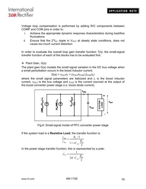
Plant Gain, G(s)<br />
The plant gain G(s) models the small signal variation in the DC bus voltage when<br />
a small perturbation occurs in the boost inductor current.<br />
G(s) = v OUT /i L = (v OUT /i CHG ).(i CHG /i L )<br />
where the small signal parameters are italicized and i L is the boost inductor<br />
current, v OUT is the bus voltage and i CHG is the current sourced at the output of<br />
the boost converter power stage (i.e. boost diode current).<br />
(2MI OUT /V OUT ).v i<br />
(V IN /kM).v m<br />
V OUT /I OUT<br />
C OUT<br />
SYSTEM<br />
LOAD<br />
R L<br />
_<br />
v OUT<br />
Fig.8: Small-signal model of PFC converter power stage<br />
If the system load is a Resistive Load, the transfer function is:<br />
vout<br />
RL<br />
/ 2<br />
=<br />
i<br />
R<br />
chg<br />
L<br />
1 + sCout<br />
2<br />
In the power stage transfer function, this is represented by a pole:<br />
1<br />
f<br />
PS<br />
=<br />
RL<br />
2π<br />
⋅Cout<br />
2<br />
www.irf.com <strong>AN</strong>-<strong>1150</strong><br />
19


