MAX9272 28-Bit GMSL Deserializer for Coax or STP Cable
MAX9272 28-Bit GMSL Deserializer for Coax or STP Cable
MAX9272 28-Bit GMSL Deserializer for Coax or STP Cable

Create successful ePaper yourself
Turn your PDF publications into a flip-book with our unique Google optimized e-Paper software.
<strong>MAX9272</strong><br />
<strong>28</strong>-<strong>Bit</strong> <strong>GMSL</strong> <strong>Deserializer</strong> <strong>f<strong>or</strong></strong> <strong>Coax</strong> <strong>or</strong> <strong>STP</strong> <strong>Cable</strong><br />
Pin Description (continued)<br />
PIN NAME FUNCTION<br />
19 DOUT24/HS0<br />
Parallel Data/H<strong>or</strong>izontal Sync 0 Output. Defaults to parallel data input on power-up.<br />
Parallel data output when VS/HS encoding is disabled.<br />
Decoded h<strong>or</strong>izontal sync <strong>f<strong>or</strong></strong> lower half of single-output when VS/HS encoding is enabled (Table 2).<br />
20, 41 IOVDD<br />
21–40,<br />
42–45<br />
DOUT23–<br />
DOUT0<br />
I/O Supply Voltage. 1.8V to 3.3V logic I/O power supply. Bypass IOVDD to EP with 0.1FF and 0.001FF<br />
capacit<strong>or</strong>s as close as possible to the device with the smallest value capacit<strong>or</strong> closest to IOVDD.<br />
Parallel Data Outputs<br />
46 PCLKOUT Parallel Clock Output. Latches parallel data into the input of another device.<br />
47 MS/HVEN<br />
— EP<br />
Mode Select/HS and VS Encoding Enable with Internal Pulldown to EP. Function is determined by the<br />
state of LCCEN (Table 13).<br />
MS (LCCEN = high). Set MS = low to select base mode. Set MS = high to select the bypass mode.<br />
HVEN (LCCEN = low): Set HVEN = high to enable HS/VS encoding on DOUT_/HS_ and DOUT_/VS_.<br />
Set HVEN = low to use DOUT_/HS_ and DOUT_/VS_ as parallel data outputs.<br />
Exposed Pad. EP is internally connected to device ground. MUST connect EP to the PCB ground<br />
plane through an array of vias <strong>f<strong>or</strong></strong> proper thermal and electrical per<strong>f<strong>or</strong></strong>mance.<br />
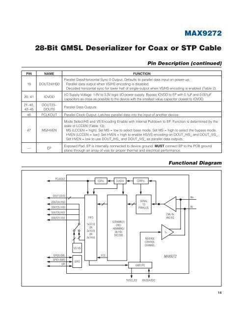
Functional Diagram<br />
PCLKOUT<br />
SSPLL CLKDIV CDRPLL<br />
DOUT [23:0]<br />
DOUT24/HS0<br />
DOUT25/ VS0<br />
SERIAL<br />
TO<br />
PARALLEL<br />
IN+<br />
IN-<br />
DOUT26/HS1<br />
DOUT27/ VS1<br />
VS /HS<br />
FIFO<br />
1x[27:0]<br />
OR<br />
2x[10:0]<br />
OR<br />
2x[14:0]<br />
SCRAMBLE/<br />
CRC/<br />
HAMMING/<br />
8b/10b<br />
DECODE<br />
REVERSE<br />
CONTROL<br />
CHANNEL<br />
CML Rx<br />
AND EQ<br />
Tx<br />
GPIO0/DBL<br />
GPIO1/BWS<br />
GPI<br />
GPIO<br />
FCC<br />
UART/I 2 C<br />
<strong>MAX9272</strong><br />
TX/SCL/ES<br />
RX/SDA/EDC<br />
14

![P-CAD EDA - [Sheet1]](https://img.yumpu.com/49470492/1/190x115/p-cad-eda-sheet1.jpg?quality=85)