MAX9272 28-Bit GMSL Deserializer for Coax or STP Cable
MAX9272 28-Bit GMSL Deserializer for Coax or STP Cable
MAX9272 28-Bit GMSL Deserializer for Coax or STP Cable

You also want an ePaper? Increase the reach of your titles
YUMPU automatically turns print PDFs into web optimized ePapers that Google loves.
<strong>MAX9272</strong><br />
<strong>28</strong>-<strong>Bit</strong> <strong>GMSL</strong> <strong>Deserializer</strong> <strong>f<strong>or</strong></strong> <strong>Coax</strong> <strong>or</strong> <strong>STP</strong> <strong>Cable</strong><br />
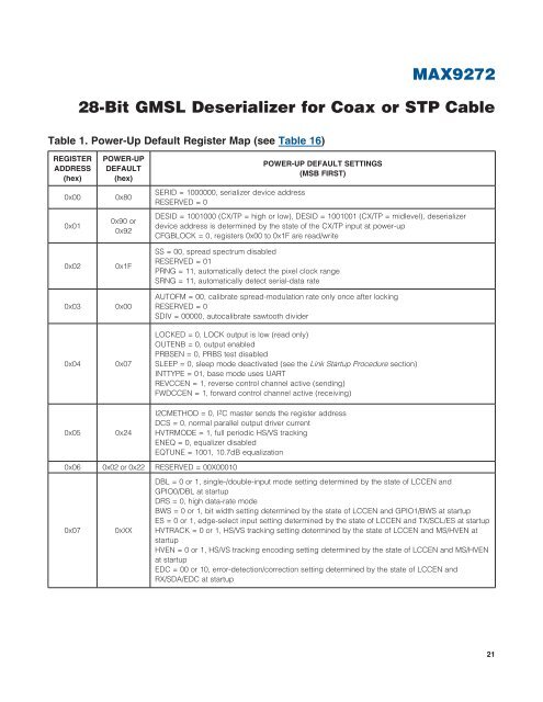
Table 1. Power-Up Default Register Map (see Table 16)<br />
REGISTER<br />
ADDRESS<br />
(hex)<br />
0x00<br />
0x01<br />
0x02<br />
0x03<br />
0x04<br />
POWER-UP<br />
DEFAULT<br />
(hex)<br />
0x80<br />
0x90 <strong>or</strong><br />
0x92<br />
0x1F<br />
0x00<br />
0x07<br />
SERID = 1000000, serializer device address<br />
RESERVED = 0<br />
POWER-UP DEFAULT SETTINGS<br />
(MSB FIRST)<br />
DESID = 1001000 (CX/TP = high <strong>or</strong> low), DESID = 1001001 (CX/TP = midlevel), deserializer<br />
device address is determined by the state of the CX/TP input at power-up<br />
CFGBLOCK = 0, registers 0x00 to 0x1F are read/write<br />
SS = 00, spread spectrum disabled<br />
RESERVED = 01<br />
PRNG = 11, automatically detect the pixel clock range<br />
SRNG = 11, automatically detect serial-data rate<br />
AUTOFM = 00, calibrate spread-modulation rate only once after locking<br />
RESERVED = 0<br />
SDIV = 00000, autocalibrate sawtooth divider<br />
LOCKED = 0, LOCK output is low (read only)<br />
OUTENB = 0, output enabled<br />
PRBSEN = 0, PRBS test disabled<br />
SLEEP = 0, sleep mode deactivated (see the Link Startup Procedure section)<br />
INTTYPE = 01, base mode uses UART<br />
REVCCEN = 1, reverse control channel active (sending)<br />
FWDCCEN = 1, <strong>f<strong>or</strong></strong>ward control channel active (receiving)<br />
0x05<br />
0x24<br />
I2CMETHOD = 0, I 2 C master sends the register address<br />
DCS = 0, n<strong>or</strong>mal parallel output driver current<br />
HVTRMODE = 1, full periodic HS/VS tracking<br />
ENEQ = 0, equalizer disabled<br />
EQTUNE = 1001, 10.7dB equalization<br />
0x06 0x02 <strong>or</strong> 0x22 RESERVED = 00X00010<br />
0x07<br />
0xXX<br />
DBL = 0 <strong>or</strong> 1, single-/double-input mode setting determined by the state of LCCEN and<br />
GPIO0/DBL at startup<br />
DRS = 0, high data-rate mode<br />
BWS = 0 <strong>or</strong> 1, bit width setting determined by the state of LCCEN and GPIO1/BWS at startup<br />
ES = 0 <strong>or</strong> 1, edge-select input setting determined by the state of LCCEN and TX/SCL/ES at startup<br />
HVTRACK = 0 <strong>or</strong> 1, HS/VS tracking setting determined by the state of LCCEN and MS/HVEN at<br />
startup<br />
HVEN = 0 <strong>or</strong> 1, HS/VS tracking encoding setting determined by the state of LCCEN and MS/HVEN<br />
at startup<br />
EDC = 00 <strong>or</strong> 10, err<strong>or</strong>-detection/c<strong>or</strong>rection setting determined by the state of LCCEN and<br />
RX/SDA/EDC at startup<br />
21

![P-CAD EDA - [Sheet1]](https://img.yumpu.com/49470492/1/190x115/p-cad-eda-sheet1.jpg?quality=85)