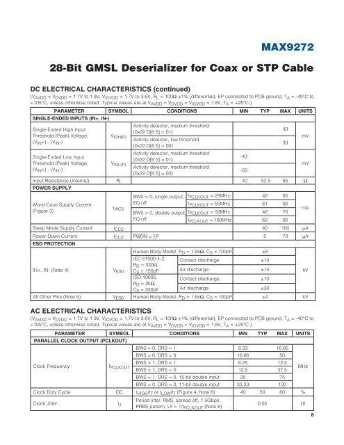
MAX9272 28-Bit GMSL Deserializer for Coax or STP Cable
MAX9272 28-Bit GMSL Deserializer for Coax or STP Cable
MAX9272 28-Bit GMSL Deserializer for Coax or STP Cable

Create successful ePaper yourself
Turn your PDF publications into a flip-book with our unique Google optimized e-Paper software.
<strong>MAX9272</strong><br />
<strong>28</strong>-<strong>Bit</strong> <strong>GMSL</strong> <strong>Deserializer</strong> <strong>f<strong>or</strong></strong> <strong>Coax</strong> <strong>or</strong> <strong>STP</strong> <strong>Cable</strong><br />
DC ELECTRICAL CHARACTERISTICS (continued)<br />
(V AVDD = V DVDD = 1.7V to 1.9V, V IOVDD = 1.7V to 3.6V, R L = 100I Q1% (differential), EP connected to PCB ground, T A = -40°C to<br />
+105°C, unless otherwise noted. Typical values are at V AVDD = V DVDD = V IOVDD = 1.8V, T A = +25°C.)<br />
PARAMETER SYMBOL CONDITIONS MIN TYP MAX UNITS<br />
SINGLE-ENDED INPUTS (IN+, IN-)<br />
Single-Ended High Input<br />
Threshold (Peak) Voltage,<br />
(V IN +) - (V IN -)<br />
Single-Ended Low Input<br />
Threshold (Peak) Voltage,<br />
(V IN +) - (V IN -)<br />
V IDH(P)<br />
V IDL(P)<br />
Activity detect<strong>or</strong>, medium threshold<br />
(0x22 D[6:5] = 01)<br />
Activity detect<strong>or</strong>, low threshold<br />
(0x22 D[6:5] = 00)<br />
Activity detect<strong>or</strong>, medium threshold<br />
(0x22 D[6:5] = 01)<br />
Activity detect<strong>or</strong>, medium threshold<br />
(0x22 D[6:5] = 00)<br />
Input Resistance (Internal) R I 40 52.5 65 I<br />
POWER SUPPLY<br />
W<strong>or</strong>st-Case Supply Current<br />
(Figure 3)<br />
I WCS<br />
BWS = 0, single output,<br />
EQ off<br />
BWS = 0, double output,<br />
EQ off<br />
AC ELECTRICAL CHARACTERISTICS<br />
(V AVDD = V DVDD = 1.7V to 1.9V, V IOVDD = 1.7V to 3.6V, R L = 100I Q1% (differential), EP connected to PCB ground, T A = -40°C to<br />
+105°C, unless otherwise noted. Typical values are at V AVDD = V DVDD = V IOVDD = 1.8V, T A = +25°C.)<br />
-43<br />
-33<br />
43<br />
33<br />
f PCLKOUT = 25MHz 42 65<br />
f PCLKOUT = 50MHz 61 90<br />
f PCLKOUT = 50MHz 42 70<br />
f PCLKOUT = 100MHz 62 90<br />
Sleep Mode Supply Current I CCS 40 100 FA<br />
Power-Down Current I CCZ PWDN = EP 5 70 FA<br />
ESD PROTECTION<br />
Human Body Model, R D = 1.5kI, C S = 100pF ±8<br />
IEC 61000-4-2, Contact discharge ±10<br />
R D = 330I,<br />
IN+, IN- (Note 4) V ESD C S = 150pF Air discharge ±15<br />
ISO 10605, Contact discharge ±10<br />
R D = 2kI,<br />
C S = 330pF Air discharge ±30<br />
All Other Pins (Note 5) V ESD Human Body Model, R D = 1.5kI, C S = 100pF ±4 kV<br />
PARAMETER SYMBOL CONDITIONS MIN TYP MAX UNITS<br />
PARALLEL CLOCK OUTPUT (PCLKOUT)<br />
Clock Frequency f PCLKOUT<br />
BWS = 1, DRS = 1 6.25 12.5<br />
BWS = 1, DRS = 0 12.5 37.5<br />
BWS = 0, DRS = 1 8.33 16.66<br />
BWS = 0, DRS = 0 16.66 50<br />
BWS = 1, DRS = 0, 15-bit double input 25 75<br />
BWS = 0, DRS = 0, 11-bit double input 33.33 100<br />
Clock Duty Cycle DC t HIGH /t T <strong>or</strong> t LOW /t T (Figure 4, Note 6) 40 50 60 %<br />
Clock Jitter t J<br />
Period jitter, RMS, spread off, 1.5Gbps,<br />
PRBS pattern, UI = 1/f PCLKOUT (Note 6)<br />
mV<br />
mV<br />
mA<br />
kV<br />
MHz<br />
0.05 UI<br />
8

![P-CAD EDA - [Sheet1]](https://img.yumpu.com/49470492/1/190x115/p-cad-eda-sheet1.jpg?quality=85)