MAX9272 28-Bit GMSL Deserializer for Coax or STP Cable
MAX9272 28-Bit GMSL Deserializer for Coax or STP Cable
MAX9272 28-Bit GMSL Deserializer for Coax or STP Cable

Create successful ePaper yourself
Turn your PDF publications into a flip-book with our unique Google optimized e-Paper software.
<strong>MAX9272</strong><br />
<strong>28</strong>-<strong>Bit</strong> <strong>GMSL</strong> <strong>Deserializer</strong> <strong>f<strong>or</strong></strong> <strong>Coax</strong> <strong>or</strong> <strong>STP</strong> <strong>Cable</strong><br />
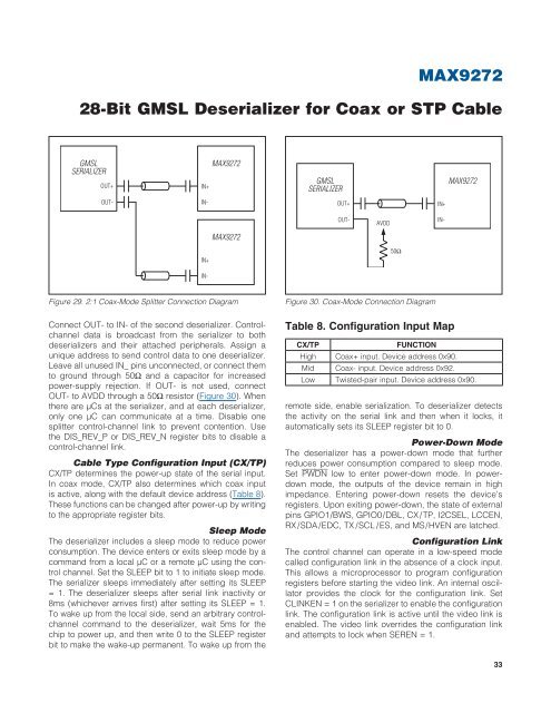
<strong>GMSL</strong><br />
SERIALIZER<br />
OUT+<br />
IN+<br />
<strong>MAX9272</strong><br />
<strong>GMSL</strong><br />
SERIALIZER<br />
<strong>MAX9272</strong><br />
OUT-<br />
IN-<br />
OUT+<br />
IN+<br />
AVDD<br />
OUT-<br />
IN-<br />
<strong>MAX9272</strong><br />
IN+<br />
50I<br />
IN-<br />
Figure 29. 2:1 <strong>Coax</strong>-Mode Splitter Connection Diagram<br />
Connect OUT- to IN- of the second deserializer. Controlchannel<br />
data is broadcast from the serializer to both<br />
deserializers and their attached peripherals. Assign a<br />
unique address to send control data to one deserializer.<br />
Leave all unused IN_ pins unconnected, <strong>or</strong> connect them<br />
to ground through 50I and a capacit<strong>or</strong> <strong>f<strong>or</strong></strong> increased<br />
power-supply rejection. If OUT- is not used, connect<br />
OUT- to AVDD through a 50I resist<strong>or</strong> (Figure 30). When<br />
there are FCs at the serializer, and at each deserializer,<br />
only one FC can communicate at a time. Disable one<br />
splitter control-channel link to prevent contention. Use<br />
the DIS_REV_P <strong>or</strong> DIS_REV_N register bits to disable a<br />
control-channel link.<br />
<strong>Cable</strong> Type Configuration Input (CX/TP)<br />
CX/TP determines the power-up state of the serial input.<br />
In coax mode, CX/TP also determines which coax input<br />
is active, along with the default device address (Table 8).<br />
These functions can be changed after power-up by writing<br />
to the appropriate register bits.<br />
Sleep Mode<br />
The deserializer includes a sleep mode to reduce power<br />
consumption. The device enters <strong>or</strong> exits sleep mode by a<br />
command from a local FC <strong>or</strong> a remote FC using the control<br />
channel. Set the SLEEP bit to 1 to initiate sleep mode.<br />
The serializer sleeps immediately after setting its SLEEP<br />
= 1. The deserializer sleeps after serial link inactivity <strong>or</strong><br />
8ms (whichever arrives first) after setting its SLEEP = 1.<br />
To wake up from the local side, send an arbitrary controlchannel<br />
command to the deserializer, wait 5ms <strong>f<strong>or</strong></strong> the<br />
chip to power up, and then write 0 to the SLEEP register<br />
bit to make the wake-up permanent. To wake up from the<br />
Figure 30. <strong>Coax</strong>-Mode Connection Diagram<br />
Table 8. Configuration Input Map<br />
CX/TP<br />
FUNCTION<br />
High <strong>Coax</strong>+ input. Device address 0x90.<br />
Mid <strong>Coax</strong>- input. Device address 0x92.<br />
Low Twisted-pair input. Device address 0x90.<br />
remote side, enable serialization. To deserializer detects<br />
the activity on the serial link and then when it locks, it<br />
automatically sets its SLEEP register bit to 0.<br />
Power-Down Mode<br />
The deserializer has a power-down mode that further<br />
reduces power consumption compared to sleep mode.<br />
Set PWDN low to enter power-down mode. In powerdown<br />
mode, the outputs of the device remain in high<br />
impedance. Entering power-down resets the device’s<br />
registers. Upon exiting power-down, the state of external<br />
pins GPIO1/BWS, GPIO0/DBL, CX/TP, I2CSEL, LCCEN,<br />
RX /SDA/EDC, TX /SCL /ES, and MS/HVEN are latched.<br />
Configuration Link<br />
The control channel can operate in a low-speed mode<br />
called configuration link in the absence of a clock input.<br />
This allows a microprocess<strong>or</strong> to program configuration<br />
registers be<strong>f<strong>or</strong></strong>e starting the video link. An internal oscillat<strong>or</strong><br />
provides the clock <strong>f<strong>or</strong></strong> the configuration link. Set<br />
CLINKEN = 1 on the serializer to enable the configuration<br />
link. The configuration link is active until the video link is<br />
enabled. The video link overrides the configuration link<br />
and attempts to lock when SEREN = 1.<br />
33

![P-CAD EDA - [Sheet1]](https://img.yumpu.com/49470492/1/190x115/p-cad-eda-sheet1.jpg?quality=85)