MAX9272 28-Bit GMSL Deserializer for Coax or STP Cable
MAX9272 28-Bit GMSL Deserializer for Coax or STP Cable
MAX9272 28-Bit GMSL Deserializer for Coax or STP Cable

Create successful ePaper yourself
Turn your PDF publications into a flip-book with our unique Google optimized e-Paper software.
<strong>MAX9272</strong><br />
<strong>28</strong>-<strong>Bit</strong> <strong>GMSL</strong> <strong>Deserializer</strong> <strong>f<strong>or</strong></strong> <strong>Coax</strong> <strong>or</strong> <strong>STP</strong> <strong>Cable</strong><br />
Providing a Frame Sync<br />
(Camera Applications)<br />
The GPI/GPO provides a simple solution <strong>f<strong>or</strong></strong> camera<br />
applications that require a frame sync signal from the<br />
ECU (e.g., surround-view systems). Connect the ECU<br />
frame sync signal to the GPI input, and connect the GPO<br />
output to the camera frame sync input. GPI/GPO have<br />
a typical delay of 275Fs. Skew between multiple GPI/<br />
GPO channels is 115Fs (max). If a lower skew signal is<br />
required, connect the camera’s frame sync input to one<br />
of the <strong>GMSL</strong> deserializer’s GPIOs and use an I 2 C broadcast<br />
write command to change the GPIO output state.<br />
This has a maximum skew of 1.5Fs.<br />
Software Programming<br />
of the Device Addresses<br />
Both the serializer and the deserializer have programmable<br />
device addresses. This allows multiple <strong>GMSL</strong><br />
devices, along with I 2 C peripherals, to coexist on the<br />
same control channel. The serializer device address<br />
is in register 0x00 of each device, while the deserializer<br />
device address is in register 0x01 of each device.<br />
To change a device address, first write to the device<br />
whose address changes (register 0x00 of the serializer<br />
<strong>f<strong>or</strong></strong> serializer device address change, <strong>or</strong> register 0x01 of<br />
the deserializer <strong>f<strong>or</strong></strong> deserializer device address change).<br />
Then write the same address into the c<strong>or</strong>responding register<br />
on the other device (register 0x00 of the deserializer<br />
<strong>f<strong>or</strong></strong> serializer device address change, <strong>or</strong> register 0x01 of<br />
the serializer <strong>f<strong>or</strong></strong> deserializer device address change).<br />
Three-Level Configuration Inputs<br />
CX/TP is a three-level input that controls the serialinterface<br />
configuration and power-up defaults. Connect<br />
CX/TP through a pullup resist<strong>or</strong> to IOVDD to set a high<br />
level, a pulldown resist<strong>or</strong> to GND to set a low level, <strong>or</strong><br />
IOVDD/2 <strong>or</strong> open to set a midlevel. F<strong>or</strong> digital control,<br />
use three-state logic to drive the three-level logic input.<br />
Configuration Blocking<br />
The deserializer can block changes to registers. Set<br />
CFGBLOCK to make all registers read only. Once set,<br />
the registers remain blocked until the supplies are<br />
removed <strong>or</strong> until PWDN is low.<br />
Compatibility with other <strong>GMSL</strong> Devices<br />
The <strong>MAX9272</strong>/MAX9273 deserializers are designed to<br />
pair with the MAX9271/MAX9273 serializers, but interoperate<br />
with any <strong>GMSL</strong> serializers. See the Table 11 <strong>f<strong>or</strong></strong><br />
operating limitations.<br />
GPIOs<br />
The deserializer has two open-drain GPIOs available<br />
when not used as configuration inputs. GPIO1OUT and<br />
GPIO0OUT (0x0E, D3 and D1) set the output state of the<br />
GPIOs. Setting the GPIO output bits to 0 pulls the output<br />
low, while setting the bits to 1 leaves the output undriven<br />
and pulled high through internal/external pullup resist<strong>or</strong>s.<br />
The GPIO input buffers are always enabled. The input<br />
states are st<strong>or</strong>ed in GPIO1 and GPIO0 (0x0E, D2 and<br />
D0). Set GPIO1OUT/GPIO0OUT to 1 when using GPIO1/<br />
GPIO0 as an input.<br />
Staggered Parallel Outputs<br />
The deserializer staggers the parallel data outputs to<br />
reduce EMI and noise. Staggering outputs also reduces<br />
the power-supply transient requirements. By default, the<br />
deserializer staggers outputs acc<strong>or</strong>ding to Table 12.<br />
Disable output staggering through the DISSTAG bit<br />
(0x08, D3).<br />
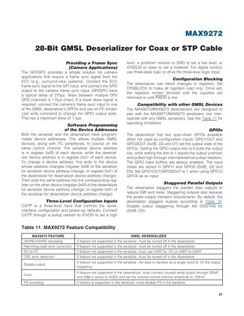
Table 11. <strong>MAX9272</strong> Feature Compatibility<br />
<strong>MAX9272</strong> FEATURE<br />
HSYNC/VSYNC encoding<br />
Hamming-code err<strong>or</strong> c<strong>or</strong>rection<br />
I 2 C-to-I 2 C<br />
CRC err<strong>or</strong> detection<br />
Double output<br />
<strong>Coax</strong><br />
I 2 S encoding<br />
<strong>GMSL</strong> DESERIALIZER<br />
If feature not supp<strong>or</strong>ted in the serializer, must be turned off in the deserializer.<br />
If feature not supp<strong>or</strong>ted in the serializer, must be turned off in the deserializer.<br />
If feature not supp<strong>or</strong>ted in the serializer, must use UART-to- I 2 C <strong>or</strong> UART-to-UART.<br />
If feature not supp<strong>or</strong>ted in the serializer, must be turned off in the deserializer.<br />
If feature not supp<strong>or</strong>ted in the serializer, the data is inputted as a single w<strong>or</strong>d at 1/2 the output<br />
frequency.<br />
If feature not supp<strong>or</strong>ted in the deserializer, must connect unused serial output through 200nF<br />
and 50I in series to AVDD and set the reverse control-channel amplitude to 100mV.<br />
If feature is supp<strong>or</strong>ted in the serializer, must disable I 2 S in the serializer.<br />
37

![P-CAD EDA - [Sheet1]](https://img.yumpu.com/49470492/1/190x115/p-cad-eda-sheet1.jpg?quality=85)