MAX9272 28-Bit GMSL Deserializer for Coax or STP Cable
MAX9272 28-Bit GMSL Deserializer for Coax or STP Cable
MAX9272 28-Bit GMSL Deserializer for Coax or STP Cable

Create successful ePaper yourself
Turn your PDF publications into a flip-book with our unique Google optimized e-Paper software.
<strong>MAX9272</strong><br />
<strong>28</strong>-<strong>Bit</strong> <strong>GMSL</strong> <strong>Deserializer</strong> <strong>f<strong>or</strong></strong> <strong>Coax</strong> <strong>or</strong> <strong>STP</strong> <strong>Cable</strong><br />
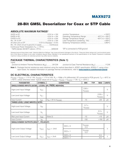
ABSOLUTE MAXIMUM RATINGS*<br />
AVDD to EP...........................................................-0.5V to +1.9V<br />
DVDD to EP...........................................................-0.5V to +1.9V<br />
IOVDD to EP..........................................................-0.5V to +3.9V<br />
IN+, IN- to EP........................................................-0.5V to +1.9V<br />
All other pins to EP..............................-0.5V to (VIOVDD + 0.5V)<br />
IN+, IN- sh<strong>or</strong>t circuit to ground <strong>or</strong> supply .................Continuous<br />
Continuous Power Dissipation (T A = +70°C)<br />
TQFN (derate 40mW/°C above +70°C).......................3200mW<br />
Junction Temperature......................................................+150°C<br />
Operating Temperature Range......................... -40°C to +105°C<br />
St<strong>or</strong>age Temperature Range............................. -65°C to +150°C<br />
Lead Temperature (soldering, 10s).................................+300°C<br />
Soldering Temperature (reflow).......................................+260°C<br />
*EP is connected to PCB ground.<br />
Stresses beyond those listed under “Absolute Maximum Ratings” may cause permanent damage to the device. These are stress ratings only, and functional operation<br />
of the device at these <strong>or</strong> any other conditions beyond those indicated in the operational sections of the specifications is not implied. Exposure to absolute<br />
maximum rating conditions <strong>f<strong>or</strong></strong> extended periods may affect device reliability.<br />
PACKAGE THERMAL CHARACTERISTICS (Note 1)<br />
TQFN<br />
Junction-to-Ambient Thermal Resistance (B JA ).............25°C/W<br />
Junction-to-Case Thermal Resistance (B JC )......................1°C/W<br />
Note 1: Package thermal resistances were obtained using the method described in JEDEC specification JESD51-7, using a fourlayer<br />
board. F<strong>or</strong> detailed in<strong>f<strong>or</strong></strong>mation on package thermal considerations, refer to www.maxim-ic.com/thermal-tut<strong>or</strong>ial.<br />
DC ELECTRICAL CHARACTERISTICS<br />
(V AVDD = V DVDD = 1.7V to 1.9V, V IOVDD = 1.7V to 3.6V, R L = 100I Q1% (differential), EP connected to PCB ground, T A = -40°C to<br />
+105°C, unless otherwise noted. Typical values are at V AVDD = V DVDD = V IOVDD = 1.8V, T A = +25°C.)<br />
PARAMETER SYMBOL CONDITIONS MIN TYP MAX UNITS<br />
SINGLE-ENDED INPUTS (I2CSEL, LCCEN, GPI, PWDN, MS/HVEN)<br />
High-Level Input Voltage V IH1<br />
0.65 x<br />
V IOVDD<br />
V<br />
Low-Level Input Voltage V IL1<br />
0.35 x<br />
V IOVDD<br />
V<br />
Input Current I IN1 V IN = 0V to V IOVDD -10 +20 FA<br />
THREE-LEVEL LOGIC INPUTS (CX/TP)<br />
High-Level Input Voltage V IH<br />
0.7 x<br />
V IOVDD<br />
V<br />
Low-Level Input Voltage V IL<br />
0.3 x<br />
V IOVDD<br />
V<br />
Mid-Level Input Current I INM (Note 2) -10 +10 FA<br />
Input Current I IN -150 +150 FA<br />
SINGLE-ENDED OUTPUTS (DOUT_, PCLKOUT)<br />
High-Level Output Voltage V OH1 I OUT = -2mA<br />
Low-Level Output Voltage V OL1 I OUT = 2mA<br />
DCS = 0<br />
DCS = 1<br />
V IOVDD<br />
- 0.3<br />
V IOVDD<br />
- 0.2<br />
DCS = 0 0.3<br />
DCS = 1 0.2<br />
V<br />
V<br />
6

![P-CAD EDA - [Sheet1]](https://img.yumpu.com/49470492/1/190x115/p-cad-eda-sheet1.jpg?quality=85)