MAX9272 28-Bit GMSL Deserializer for Coax or STP Cable
MAX9272 28-Bit GMSL Deserializer for Coax or STP Cable
MAX9272 28-Bit GMSL Deserializer for Coax or STP Cable

Create successful ePaper yourself
Turn your PDF publications into a flip-book with our unique Google optimized e-Paper software.
<strong>MAX9272</strong><br />
<strong>28</strong>-<strong>Bit</strong> <strong>GMSL</strong> <strong>Deserializer</strong> <strong>f<strong>or</strong></strong> <strong>Coax</strong> <strong>or</strong> <strong>STP</strong> <strong>Cable</strong><br />
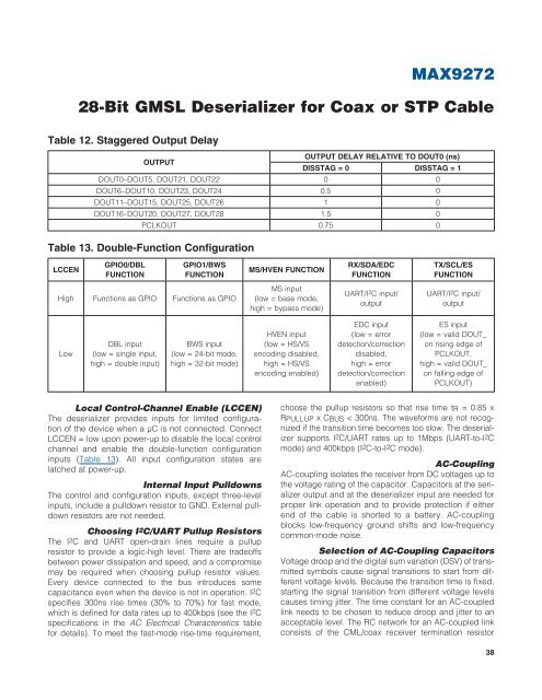
Table 12. Staggered Output Delay<br />
OUTPUT<br />
OUTPUT DELAY RELATIVE TO DOUT0 (ns)<br />
DISSTAG = 0 DISSTAG = 1<br />
DOUT0–DOUT5, DOUT21, DOUT22 0 0<br />
DOUT6–DOUT10, DOUT23, DOUT24 0.5 0<br />
DOUT11–DOUT15, DOUT25, DOUT26 1 0<br />
DOUT16–DOUT20, DOUT27, DOUT<strong>28</strong> 1.5 0<br />
PCLKOUT 0.75 0<br />
Table 13. Double-Function Configuration<br />
LCCEN<br />
GPIO0/DBL<br />
FUNCTION<br />
GPIO1/BWS<br />
FUNCTION<br />
MS/HVEN FUNCTION<br />
RX/SDA/EDC<br />
FUNCTION<br />
TX/SCL/ES<br />
FUNCTION<br />
High Functions as GPIO Functions as GPIO<br />
MS input<br />
(low = base mode,<br />
high = bypass mode)<br />
UART/I 2 C input/<br />
output<br />
UART/I 2 C input/<br />
output<br />
Low<br />
DBL input<br />
(low = single input,<br />
high = double input)<br />
BWS input<br />
(low = 24-bit mode,<br />
high = 32-bit mode)<br />
HVEN input<br />
(low = HS/VS<br />
encoding disabled,<br />
high = HS/VS<br />
encoding enabled)<br />
EDC input<br />
(low = err<strong>or</strong><br />
detection/c<strong>or</strong>rection<br />
disabled,<br />
high = err<strong>or</strong><br />
detection/c<strong>or</strong>rection<br />
enabled)<br />
ES input<br />
(low = valid DOUT_<br />
on rising edge of<br />
PCLKOUT,<br />
high = valid DOUT_<br />
on falling edge of<br />
PCLKOUT)<br />
Local Control-Channel Enable (LCCEN)<br />
The deserializer provides inputs <strong>f<strong>or</strong></strong> limited configuration<br />
of the device when a FC is not connected. Connect<br />
LCCEN = low upon power-up to disable the local control<br />
channel and enable the double-function configuration<br />
inputs (Table 13). All input configuration states are<br />
latched at power-up.<br />
Internal Input Pulldowns<br />
The control and configuration inputs, except three-level<br />
inputs, include a pulldown resist<strong>or</strong> to GND. External pulldown<br />
resist<strong>or</strong>s are not needed.<br />
Choosing I 2 C/UART Pullup Resist<strong>or</strong>s<br />
The I 2 C and UART open-drain lines require a pullup<br />
resist<strong>or</strong> to provide a logic-high level. There are tradeoffs<br />
between power dissipation and speed, and a compromise<br />
may be required when choosing pullup resist<strong>or</strong> values.<br />
Every device connected to the bus introduces some<br />
capacitance even when the device is not in operation. I 2 C<br />
specifies 300ns rise times (30% to 70%) <strong>f<strong>or</strong></strong> fast mode,<br />
which is defined <strong>f<strong>or</strong></strong> data rates up to 400kbps (see the I 2 C<br />
specifications in the AC Electrical Characteristics table<br />
<strong>f<strong>or</strong></strong> details). To meet the fast-mode rise-time requirement,<br />
choose the pullup resist<strong>or</strong>s so that rise time tR = 0.85 x<br />
RPULLUP x CBUS < 300ns. The wave<strong>f<strong>or</strong></strong>ms are not recognized<br />
if the transition time becomes too slow. The deserializer<br />
supp<strong>or</strong>ts I 2 C/UART rates up to 1Mbps (UART-to-I 2 C<br />
mode) and 400kbps (I 2 C-to-I 2 C mode).<br />
AC-Coupling<br />
AC-coupling isolates the receiver from DC voltages up to<br />
the voltage rating of the capacit<strong>or</strong>. Capacit<strong>or</strong>s at the serializer<br />
output and at the deserializer input are needed <strong>f<strong>or</strong></strong><br />
proper link operation and to provide protection if either<br />
end of the cable is sh<strong>or</strong>ted to a battery. AC-coupling<br />
blocks low-frequency ground shifts and low-frequency<br />
common-mode noise.<br />
Selection of AC-Coupling Capacit<strong>or</strong>s<br />
Voltage droop and the digital sum variation (DSV) of transmitted<br />
symbols cause signal transitions to start from different<br />
voltage levels. Because the transition time is fixed,<br />
starting the signal transition from different voltage levels<br />
causes timing jitter. The time constant <strong>f<strong>or</strong></strong> an AC-coupled<br />
link needs to be chosen to reduce droop and jitter to an<br />
acceptable level. The RC netw<strong>or</strong>k <strong>f<strong>or</strong></strong> an AC-coupled link<br />
consists of the CML/coax receiver termination resist<strong>or</strong><br />
38

![P-CAD EDA - [Sheet1]](https://img.yumpu.com/49470492/1/190x115/p-cad-eda-sheet1.jpg?quality=85)