MAX9272 28-Bit GMSL Deserializer for Coax or STP Cable
MAX9272 28-Bit GMSL Deserializer for Coax or STP Cable
MAX9272 28-Bit GMSL Deserializer for Coax or STP Cable

You also want an ePaper? Increase the reach of your titles
YUMPU automatically turns print PDFs into web optimized ePapers that Google loves.
<strong>MAX9272</strong><br />
<strong>28</strong>-<strong>Bit</strong> <strong>GMSL</strong> <strong>Deserializer</strong> <strong>f<strong>or</strong></strong> <strong>Coax</strong> <strong>or</strong> <strong>STP</strong> <strong>Cable</strong><br />
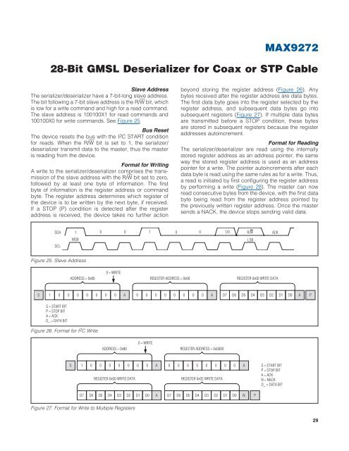
Slave Address<br />
The serializer/deserializer have a 7-bit-long slave address.<br />
The bit following a 7-bit slave address is the R/W bit, which<br />
is low <strong>f<strong>or</strong></strong> a write command and high <strong>f<strong>or</strong></strong> a read command.<br />
The slave address is 100100X1 <strong>f<strong>or</strong></strong> read commands and<br />
100100X0 <strong>f<strong>or</strong></strong> write commands. See Figure 25.<br />
Bus Reset<br />
The device resets the bus with the I 2 C START condition<br />
<strong>f<strong>or</strong></strong> reads. When the R/W bit is set to 1, the serializer/<br />
deserializer transmit data to the master, thus the master<br />
is reading from the device.<br />
F<strong>or</strong>mat <strong>f<strong>or</strong></strong> Writing<br />
A write to the serializer/deserializer comprises the transmission<br />
of the slave address with the R/W bit set to zero,<br />
followed by at least one byte of in<strong>f<strong>or</strong></strong>mation. The first<br />
byte of in<strong>f<strong>or</strong></strong>mation is the register address <strong>or</strong> command<br />
byte. The register address determines which register of<br />
the device is to be written by the next byte, if received.<br />
If a STOP (P) condition is detected after the register<br />
address is received, the device takes no further action<br />
beyond st<strong>or</strong>ing the register address (Figure 26). Any<br />
bytes received after the register address are data bytes.<br />
The first data byte goes into the register selected by the<br />
register address, and subsequent data bytes go into<br />
subsequent registers (Figure 27). If multiple data bytes<br />
are transmitted be<strong>f<strong>or</strong></strong>e a STOP condition, these bytes<br />
are st<strong>or</strong>ed in subsequent registers because the register<br />
addresses autoincrement.<br />
F<strong>or</strong>mat <strong>f<strong>or</strong></strong> Reading<br />
The serializer/deserializer are read using the internally<br />
st<strong>or</strong>ed register address as an address pointer, the same<br />
way the st<strong>or</strong>ed register address is used as an address<br />
pointer <strong>f<strong>or</strong></strong> a write. The pointer autoincrements after each<br />
data byte is read using the same rules as <strong>f<strong>or</strong></strong> a write. Thus,<br />
a read is initiated by first configuring the register address<br />
by per<strong>f<strong>or</strong></strong>ming a write (Figure <strong>28</strong>). The master can now<br />
read consecutive bytes from the device, with the first data<br />
byte being read from the register address pointed by<br />
the previously written register address. Once the master<br />
sends a NACK, the device stops sending valid data.<br />
SDA 1 0 0 1 0 0 1/0 R/W ACK<br />
MSB<br />
LSB<br />
SCL<br />
Figure 25. Slave Address<br />
ADDRESS = 0x80<br />
0 = WRITE<br />
REGISTER ADDRESS = 0x00<br />
REGISTER 0x00 WRITE DATA<br />
S 1 0 0 0<br />
0 0 0 0 A 0 0 0 0<br />
0 0 0 0 A D7 D6 D5 D4 D3 D2 D1 D0 A P<br />
S = START BIT<br />
P = STOP BIT<br />
A = ACK<br />
D_ = DATA BIT<br />
Figure 26. F<strong>or</strong>mat <strong>f<strong>or</strong></strong> I 2 C Write<br />
ADDRESS = 0x80<br />
0 = WRITE<br />
REGISTER ADDRESS = 0x0000<br />
S 1 0 0 0 0 0 0 0 A 0 0 0 0 0 0 0 0 A<br />
REGISTER 0x00 WRITE DATA<br />
REGISTER 0x02 WRITE DATA<br />
S = START BIT<br />
P = STOP BIT<br />
A = ACK<br />
N = NACK<br />
D_ = DATA BIT<br />
D7 D6 D5 D4<br />
D3 D2 D1 D0 A D7 D6 D5 D4 D3 D2 D1 D0 N P<br />
Figure 27. F<strong>or</strong>mat <strong>f<strong>or</strong></strong> Write to Multiple Registers<br />
29

![P-CAD EDA - [Sheet1]](https://img.yumpu.com/49470492/1/190x115/p-cad-eda-sheet1.jpg?quality=85)