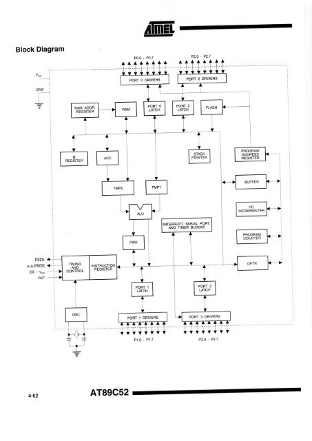
A I1M, Block Diagram Vcc GND RAM ADDR. REGISTER RAM P0.0 - P0.7 PORT 0 DRIVERS I PORT 0 I LATCH P2.0 - P2.7 • • • • ••• • • * • • 4/ • • PORT 2 DRIVERS • # PORT 2 FLASH LATCH 14 I REGISTER I ACC STACK POINTER I PROGRAM ADDRESS REGISTER • • TMP2 TMP1 BUFFER PSW ALU I INTERRUPT SERIAL PORT, AND TIMER BLOCKS • 1 PC INCREMENTER 11 PROGRAM 14_ COUNTER PSEN ALE/PROG EA / V p, TIMING AND CONTROL INSTRUCTION REGISTER DPTR RST 00% PORT 1 LATCH PORT 3 LATCH OSC PORT 1 DRIVERS PORT 3 DRIVERS • • • Ilk_ • • P1.0 - P1.7 4' • • * ♦ * • P3.0 - P3.7 4-62 AT89C52
AT89C52 The AT89C52 provi<strong>de</strong>s the following standard features: 8K bytes of Flash, 256 bytes of RAM, 32 I/O lines, three 16-bit timer/counters, a six-vector two-level interrupt architecture, a full duplex serial port, on-chip oscillator, and clock circuitry. In addition, the AT89C52 is <strong>de</strong>signed with static logic for operation down to zero frequency and supports two software selectable power saving mo<strong>de</strong>s. The Idle Mo<strong>de</strong> stops the CPU while allowing the RAM, timer/counters, serial port, and interrupt system to continue functioning. The Power Down Mo<strong>de</strong> saves the RAM contents but freezes the oscillator, disabling all other chip functions until the next hardware reset. Pin Description Vcc Supply voltage. GND Ground. Port 0 Port 0 is an 8-bit open drain bidirectional I/O port. As an output port, each pin can sink eight TTL inputs. When 1s are written to port 0 pins, the pins can be used as highimpedance inputs. Port 0 can also be configured to be the multiplexed lowor<strong>de</strong>r address/data bus during accesses to external program and data memory. In this mo<strong>de</strong>, PO has internal pullups. Port 0 also receives the co<strong>de</strong> bytes during Flash programming and outputs the co<strong>de</strong> bytes during program verification. External pullups are required during program verification. Port 1 Port 1 is an 8-bit bidirectional I/O port with internal pullups. The Port 1 output buffers can sink/source four TTL inputs. When 1s are written to Port 1 pins, they are pulled high by the internal pullups and can be used as inputs. As inputs, Port 1 pins that are externally being pulled low will source current (I L) because of the internal pullups. In addition, P1.0 and P1.1 can be configured to be the timer/counter 2 external count input (P1.0/T2) and the timer/counter 2 trigger input (P1.1/T2EX), respectively, as shown in the following table. Port 1 also receives the low-or<strong>de</strong>r address bytes during ro rammin _ and verification. Port Pin Alternate Functions P1.0 T2 (external count input to Timer/Counter 2), clock-out P1.1 T2EX (Timer/Counter 2 capture/reload trigger and direction control) Port 2 Port 2 is an 8-bit bidirectional I/O port with internal pullups. The Port 2 output buffers can sink/source four TTL inputs. When 1s are written to Port 2 pins, they are pulled high by the internal pullups and can be used as inputs. As inputs, Port 2 pins that are externally being pulled low will source current (I L) because of the internal pullups. Port 2 emits the high-or<strong>de</strong>r address byte during fetches from external program memory and during accesses to external data memory that use 16-bit addresses (MOVX @ DPTR). In this application, Port 2 uses strong internal pullups when emitting 1s. During accesses to external data memory that use 8-bit addresses (MOVX @ RI), Port 2 emits the contents of the P2 Special Function Register. Port 2 also receives the high-or<strong>de</strong>r address bits and some control signals during Flash programming and verification. Port 3 Port 3 is an 8-bit bidirectional I/O port with internal pullups. The Port 3 output buffers can sink/source four TTL inputs. When 1s are written to Port 3 pins, they are pulled high by the internal pullups and can be used as inputs. As inputs, Port 3 pins that are externally being pulled low will source current (l ip) because of the pullups. Port 3 also serves the functions of various special features of the AT89C51, as shown in the following table. Port 3 also receives some control signals for Flash promin .., and verification. . Port Pin Alternate Functions P3.0 RXD (serial input port) P3.1 TXD (serial output port) P3.2 INTO (external interrupt 0) P3.3 INT1 (external interrupt 1) P3.4 TO (timer 0 external input) P3.5 T1 (timer 1 external input) P3.6 WR (external data memory write strobe) P3.7 RD (external data memory read strobe) RST Reset input. A high on this pin for two machine cycles while the oscillator is running resets the <strong>de</strong>vice. ALE/PROG Address Latch Enable is an output pulse for latching the low byte of the address during accesses to external memory. This pin is also the program pulse input (PROG) during Flash programming. In normal operation, ALE is emitted at a constant rate of 1/6 the oscillator frequency and may be used for external timing or clocking purposes. Note, however, that one ALE 4-63
- Page 1 and 2:
F224d Faria, Rubens Alexandre de De
- Page 3 and 4:
7. COMPONENTE: TITULAcA0(siGLA): IN
- Page 5 and 6:
CADASTRO DE PROFESSOR DE OUTRA INST
- Page 7 and 8:
TESES / INFORMAQOES AREA DE CONHECI
- Page 9 and 10:
RUBENS ALEXANDRE DE FARIA DESENVOLV
- Page 11 and 12:
E finalmente o espaco reservado aos
- Page 13 and 14:
2.12 INFLUENIA DE OUTROS FATORES Fi
- Page 15 and 16:
ANEXO IV DIAGRAMAS ESQUEMATICOS 95
- Page 17 and 18:
Figura 3 Desenho de uma incubadora
- Page 19 and 20:
LISTA DE TABELAS Tabela 1 Temperatu
- Page 21 and 22:
ABSTRACT In this work it is describ
- Page 23 and 24:
2 em modificar as condicoes ambient
- Page 25 and 26:
4 Neste capitulo foram apresentados
- Page 27 and 28:
6 A incubadora dotada de controle a
- Page 29 and 30:
8 penla de calor perda (le calor se
- Page 31 and 32:
10 coeficiente varia de acordo corn
- Page 33 and 34:
12 2.7.1 HIPERTERMIA A hipertermia
- Page 35 and 36:
14 A medida adquirida no sensor de
- Page 37 and 38:
16 incubadora para que a potencia s
- Page 39 and 40:
18 parede do equipamento. Desse mod
- Page 41 and 42:
20 Tabela 1 - Temperatura da incuba
- Page 43 and 44:
22 de 80 dB (FANAROFF & KLAUS, 1995
- Page 45 and 46:
CAPITULO 3 A CERTIFICAcAO DO EQUIPA
- Page 47 and 48:
26 Segundo o INMETRO (Instituto Nac
- Page 49 and 50:
28 10/03/1998. 0 OCP deve assegurar
- Page 51 and 52:
30 A rede eletrica de 127 ou 220 V
- Page 53 and 54:
32 0 modo de controle termico da in
- Page 55 and 56:
34 sonoro. A indicacao visual deve
- Page 57 and 58:
36 A norma NBR IEC 601-2-19 equipam
- Page 59 and 60:
38 tipos de reuniao, confeccionando
- Page 61 and 62:
40 ALTMENTACAO GERADOR RESET BARRAM
- Page 63 and 64:
42 0 diagrama esquematico correspon
- Page 65 and 66:
44 a escala atraves de potenciometr
- Page 67 and 68:
46 Urn byte de controle e o primeir
- Page 69 and 70:
48 0 maior problema dos sensores qu
- Page 71 and 72: 50 A saida do sensor HC600 fornece
- Page 73 and 74: 52 4.3.4.2 DISPLAY DE CRISTAL LIQUI
- Page 75 and 76: 54 4.3.4.3 CONTROLE DE TEMPERATURA
- Page 77 and 78: 56 CONSTMAIS: DB 00H,10H,F2H,DOH DB
- Page 79 and 80: 58 (a) 4-+ 5mskliv 2V1div (b) 5ms/d
- Page 81 and 82: 60 4.3.5 ALARMES E ATUADORES 4.3.5.
- Page 83 and 84: 62 ar, pelo menos 3 minutos ap6s o
- Page 85 and 86: 64 esta tarefa pois cada temperatur
- Page 87 and 88: 66 0 tempo para aquecer a incubador
- Page 89 and 90: 68 ma tambem esta entre os sensores
- Page 91 and 92: 70 almente e seria especifico para
- Page 93 and 94: CAPITULO 6 DISCUSSAO GERAL E CONCLU
- Page 95 and 96: 74 Um problema que deve ser resolvi
- Page 97 and 98: 76 ANEXO I LABORATORIOS CREDENCIADO
- Page 99 and 100: 78 ANEXO II TOPICOS DA NORMA TECNIC
- Page 101 and 102: 80 Temperatura de Controle: Tempera
- Page 103 and 104: 82 IDENTIFICAcAO, MARCACAO E DOCUME
- Page 105 and 106: 84 SEcA0 SETE - PROTE00 CONTRA TEMP
- Page 107 and 108: 86 SEcA0 OITO - EXATIDAO NOS DADOS
- Page 109 and 110: 88 tensao nominal e o equipamento o
- Page 111 and 112: 90 - Onde urn movimento relativo de
- Page 113 and 114: 92 - Na utilizacao normal, a veloci
- Page 115 and 116: 94 CRONOGRAMA DE ATIVIDADES PARA 0
- Page 117 and 118: W gEtq 1 w f 2 8 g .11 IF 2 0 CO MU
- Page 119 and 120: ID —• 0) 1° 1• O C 03 LI N.)
- Page 121: Features • Compatible with MCS-51
- Page 125 and 126: AT89C52 Special Function Registers
- Page 127 and 128: 106 ANEXO VI CARACTERISTICAS TECNIC
- Page 129 and 130: 108 tura é efetuada em 13 bits de
- Page 131 and 132: 110 ANEXO VII CARACTERISTICAS TECNI
- Page 133 and 134: 112 Tabela VII.II - Valores maximos
- Page 135 and 136: 114 ANEXO VIII FOTOS DAS PLATAFORMA
- Page 137 and 138: 116 Figura VIII.III - Hardware fina
- Page 139 and 140: 118 Figura VIII.VII - Incubadora em
- Page 141 and 142: 120 REFERENCIAS BIBLIOGRAFICAS 1. A
- Page 143: 122 21. SEGRE, C. A. M. RN (Recem -