F224d Faria, Rubens Alexandre de Desenvolvimento de ... - UTFPR
F224d Faria, Rubens Alexandre de Desenvolvimento de ... - UTFPR
F224d Faria, Rubens Alexandre de Desenvolvimento de ... - UTFPR

You also want an ePaper? Increase the reach of your titles
YUMPU automatically turns print PDFs into web optimized ePapers that Google loves.
AT89C52<br />
Special Function Registers<br />
A map of the on-chip memory area called the Special Function<br />
Register (SFR) space is shown in Table 1.<br />
Note that not all of the addresses are occupied, and unoccupied<br />
addresses may not be implemented on the chip.<br />
Read accesses to these addresses will in general return<br />
random data, and write accesses will have an in<strong>de</strong>termi-<br />
nate effect.<br />
User software should not write 1 s to these unlisted locations,<br />
since they may be used in future products to invoke<br />
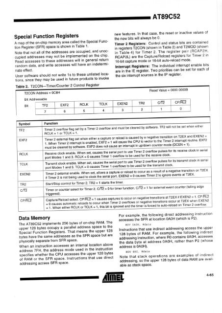
Table 2.<br />
T2CON—Timer/Counter 2 Control Register<br />
new<br />
T2CON Address = 0C8H<br />
Bit Addressable<br />
features. In that case, the reset or inactive values of<br />
the new bits will always be 0.<br />
Timer 2 Registers: Control and status bits are contained<br />
in registers T2CON (shown in Table 2) and T2MOD (shown<br />
in Table 4) for Timer 2. The register pair (RCAP2H,<br />
RCAP2L) are the Capture/Reload registers for Timer 2 in<br />
16-bit capture mo<strong>de</strong> or 16-bit auto-reload mo<strong>de</strong>.<br />
Interrupt Registers: The individual interrupt enable bits<br />
are in the IE register. Two priorities can be set for each of<br />
the six interrupt sources in the IP register.<br />
tinnQ<br />
n<br />
Hesei value = uvu,, ,,,,...,<br />
Bit TF2 EXF2 RCLK TCLK EXEN2 TR2 CTT2 CP/RL2<br />
7 6 5 4 3 2 1 0<br />
Symbol<br />
TF2<br />
EXF2<br />
RCLK<br />
TCLK<br />
EXEN2<br />
Function<br />
Timer 2 overflow flag set by a Timer 2 overflow and must be cleared by software. TF2 will not be set when either<br />
RCLK = 1 or TCLK = 1.<br />
Timer 2 external flag set when either a capture or reload is caused by a negative transition on T2EX and EXEN2 =<br />
1. When Timer 2 interrupt is enabled, EXF2 = 1 will cause the CPU to vector to the Timer 2 interrupt routine. EXF2<br />
must be cleared by software. EXF2 does not cause an interrupt in up/down counter mo<strong>de</strong> (DCEN = 1).<br />
Receive clock enable. When set, causes the serial port to use Timer 2 overflow pulses for its receive clock in serial<br />
port Mo<strong>de</strong>s 1 and 3. RCLK = 0 causes Timer 1 overflow to be used for the receive clock.<br />
Transmit clock enable. When set, causes the serial port to use Timer 2 overflow pulses for its transmit clock in serial<br />
port Mo<strong>de</strong>s 1 and 3. TCLK = 0 causes Timer 1 overflows to be used for the transmit clock.<br />
Timer 2 external enable. When set, allows a capture or reload to occur as a result of a negative transition on T2EX<br />
if Timer 2 is not being used to clock the serial port. EXEN2 = 0 causes Timer 2 to ignore events at T2EX.<br />
TR2<br />
Start/Stop control for Timer 2. TR2 = 1 starts the timer.<br />
Cfr2 Timer or counter select for Timer 2. C a2 = 0 for timer function. C/T2 = 1 for external event counter (falling edge<br />
triggered).<br />
Capture/Reload select. CP/RL2 =1 causes captures to occur on negative transitions at T2EX if EXEN2 = 1. CP/RL2<br />
CP/R L2<br />
= 0 causes automatic reloads to occur when Timer 2 overflows or negative transitions occur at T2EX when EXEN2<br />
= 1. When either RCLK or TCLK = 1, this bit is ignored and the timer is forced to auto-reload on Timer 2 overflow.<br />
Data Memory<br />
The AT89C52 implements 256 bytes of on-chip RAM. The<br />
upper 128 bytes occupy a parallel address space to the<br />
Special Function Registers. That means the upper 128<br />
bytes have the same addresses as the SFR space but are<br />
physically separate from SFR space.<br />
When an instruction accesses an internal location above<br />
address 7FH, the address mo<strong>de</strong> used in the instruction<br />
specifies whether the CPU accesses the upper 128 bytes<br />
of RAM or the SFR space. Instructions that use direct<br />
addressing access SFR space.<br />
For example, the following direct addressing instruction<br />
accesses the SFR at location OAOH (which is P2).<br />
MOV OAOH, #data<br />
Instructions that use indirect addressing access the upper<br />
128 bytes of RAM. For example, the following indirect<br />
addressing instruction, where RO contains OAOH, accesses<br />
the data byte at address OAOH, rather than P2 (whose<br />
address is OAOH).<br />
MOV @RO, #data<br />
Note that stack operations are examples of indirect<br />
addressing, so the upper 128 bytes of data RAM are available<br />
as stack space.<br />
Neff,<br />
4-65