Dirac Fermions in Graphene and Graphiteâa view from angle ...
Dirac Fermions in Graphene and Graphiteâa view from angle ...
Dirac Fermions in Graphene and Graphiteâa view from angle ...

You also want an ePaper? Increase the reach of your titles
YUMPU automatically turns print PDFs into web optimized ePapers that Google loves.
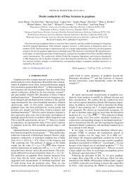
Figure 4.7. Dispersions measured <strong>in</strong> bilayer graphene on 6H-SiC (panel a) <strong>and</strong> more <strong>in</strong>sulat<strong>in</strong>g<br />
4H-SiC (panel b) substrates.<br />
consistent check for the sample thickness determ<strong>in</strong>ed by other methods 37,62 . Panel (d) shows the ARPES<br />
data taken along a l<strong>in</strong>e through the H po<strong>in</strong>t <strong>in</strong> graphite, where the dispersion resembles that of graphene<br />
through K 64 . Data shown <strong>in</strong> panels (a-d) allow us to determ<strong>in</strong>e how the electronic structure near K po<strong>in</strong>t<br />
varies as the sample thickness <strong>in</strong>creases. First of all, as the sample thickness <strong>in</strong>creases, E D shifts toward E F .<br />
From s<strong>in</strong>gle layer to trilayer graphene, E D (marked by arrows <strong>in</strong> panels (a-c)) shifts <strong>from</strong> -0.4 eV to -0.29<br />
eV then to -0.2 eV. For graphite, E D has been estimated to be at ≈0.05 eV above E F 64 . More importantly,<br />
as the sample becomes thicker, the gap (labeled by light blue shaded area <strong>in</strong> panels (a-c)) decreases rapidly.<br />
From s<strong>in</strong>gle layer to trilayer graphene, the gap decreases <strong>from</strong> 0.26 eV to 0.14 eV then to 0.066 eV. For<br />
graphite, s<strong>in</strong>ce the <strong>Dirac</strong> po<strong>in</strong>t energy is above E F 64 , whether there is a gap or not cannot be directly<br />
addressed by ARPES. However, <strong>from</strong> b<strong>and</strong> structure calculation, it is expected that the gap at the H po<strong>in</strong>t<br />
is ≈ 0.008 eV 9,74 , which is almost negligible.<br />
Fig. 4.7 shows comparison of data taken on one bilayer graphene sample on a more <strong>in</strong>sulat<strong>in</strong>g 4H-SiC<br />
substrate with resistivity of 10 5 Ω/cm (panel b) compared to another graphene sample on a 6H-SiC with<br />
resistivity of 0.2 Ω/cm (panel a). In both cases, the <strong>Dirac</strong> po<strong>in</strong>t energy appears to be shifted by a similar<br />
amount below E F , suggest<strong>in</strong>g that the dop<strong>in</strong>g is most likely associated with the surface charges at the<br />
<strong>in</strong>terface, rather than the carrier concentration of the substrate.<br />
Fig. 4.8 summarizes the evolution of the <strong>Dirac</strong> po<strong>in</strong>t energy E D <strong>and</strong> the gap ∆ for various sample<br />
thickness. The layer dependence of both quantities suggests that, beyond 5 layers, epitaxial graphene<br />
behaves as bulk graphite 64 . The amount of dop<strong>in</strong>g should decrease as the sample becomes thicker, because<br />
the surface layer probed by ARPES is farther away <strong>from</strong> the <strong>in</strong>terface as the thickness <strong>in</strong>creases. Also, the<br />
strong dependence of E D on sample thickness is a direct manifestation of the short <strong>in</strong>terlayer screen<strong>in</strong>g length<br />
(≈ 5 layers 75 ) of graphene. This result shows that the sample thickness is an effective way of controll<strong>in</strong>g<br />
dop<strong>in</strong>g <strong>in</strong> epitaxial graphene. Panel(b) shows the dependence of the gap on the sample thickness. A gap<br />
<strong>in</strong> bilayer graphene has been reported <strong>and</strong> attributed to the different potentials <strong>in</strong> the two graphene layers<br />
<strong>in</strong>duced by dop<strong>in</strong>g or electric field 76,77,78 . While this could contribute to the gap <strong>in</strong> bilayer <strong>and</strong> even trilayer<br />
graphene, it certa<strong>in</strong>ly is not the reason for the gap <strong>in</strong> the s<strong>in</strong>gle layer graphene.<br />
30