Activity Report 2010 - CNRS
Activity Report 2010 - CNRS
Activity Report 2010 - CNRS

Create successful ePaper yourself
Turn your PDF publications into a flip-book with our unique Google optimized e-Paper software.
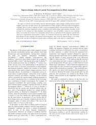
governing the formation and stability of semiconducting<br />
quantum dots, silicon nanowires and graphene sheets.<br />
<strong>2010</strong> Call for Proposals<br />
Name<br />
Nationality<br />
Duration<br />
FULL TIME<br />
Major topic Description From<br />
JoQOLaT<br />
Starting<br />
on<br />
Max<br />
HOFHEINZ<br />
3 years<br />
Quantum<br />
Nanoelectronics<br />
The new expertise in microwave quantum optics and<br />
dynamical Coulomb blockade brought by Max HOFHEINZ<br />
is at the core of this project that will include the<br />
development of various specific devices and circuits -<br />
based on his experience with superconducting quantum<br />
circuits (phase qubits and microwave resonators).<br />
IRAMIS/<br />
SPEC,<br />
CEA Saclay<br />
(France)<br />
July 2011<br />
PART TIME<br />
CORTRANO<br />
Harold<br />
BARANGER<br />
9m/3 years<br />
David<br />
GRAVES<br />
9m/3 years<br />
Nanosimulation<br />
Nanosimulation<br />
Harold BARANGER has a track record of making<br />
connections between theorists working with computational<br />
techniques and those making analytic progress. He will<br />
bring specific expertise in several computational and<br />
theoretical areas: path-integral quantum Monte Carlo<br />
simulation, molecular electronics using DFT combined with<br />
one-body Green function and in particular one of the first<br />
applications to spintronics.<br />
NSCGP<br />
This project is to benefit from the expertise of Prof. David<br />
GRAVES in the field of Molecular Dynamic Simulations<br />
applied to plasma-surface interactions. The goal is to<br />
determine under which plasma conditions graphene layers<br />
can be etched without damage. If it succeeds it will<br />
provide a technology to get the high quality samples that<br />
are required for fundamental studies of graphene<br />
properties as well as the possibility to pattern large area<br />
wafers for industrial applications.<br />
Duke<br />
University<br />
(USA)<br />
Berkeley<br />
University<br />
(USA)<br />
June<br />
2011<br />
June<br />
2011<br />
SUPPLEMENTS<br />
NISHI CHAIR<br />
Yoshio<br />
NISHI<br />
9m/3 years<br />
Nanomaterials<br />
Yoshio NISHI and his team at Stanford have a strong<br />
expertise in the field of MOS devices and technology and<br />
have made recent breakthroughs in the technology of Ge<br />
channel NMOS devices. The know-how of Prof. Nishi<br />
regarding Ge material, Metallic source and drains MOSFET<br />
will strongly benefit to the local community and will allow<br />
making significant progress in terms of technological and<br />
scientific aspects.<br />
Stanford<br />
University<br />
(USA)<br />
April<br />
2011<br />
3D-CDI<br />
Jian-Min<br />
ZUO<br />
9m/3 years<br />
Nanocharacterisation<br />
At University of Illinois, Prof. Jian Min ZUO has dedicated<br />
the past 8 years on the development of electron Coherent<br />
Diffractive Imaging (CDI) for structure characterization of<br />
nanoparticles and carbon nanotubes. This project on<br />
semiconductor, oxide nanowires, and organic<br />
nanostructures provides a further opportunity to broaden<br />
the application of electron CDI and to improve 3D<br />
coherent diffractive imaging with comparison with<br />
synchrotron.<br />
University<br />
of Illinois<br />
(USA)<br />
May<br />
2011<br />
15