Activity Report 2010 - CNRS
Activity Report 2010 - CNRS
Activity Report 2010 - CNRS

Create successful ePaper yourself
Turn your PDF publications into a flip-book with our unique Google optimized e-Paper software.
CRISTAL PHASE<br />
TRANSITIONS IN<br />
PRESSURIZED SILICON<br />
NANOWIRES<br />
The possibility to synthesize new<br />
crystalline phases in single silicon<br />
nanowires recently attracted attention<br />
owing to the potential tuning of the opto<br />
electronic properties that can be expected<br />
when the crystal structure undergoes<br />
phase transitions. In particular, it is<br />
predicted that the wurtzite phase which is<br />
metastable at room pressure and<br />
temperature is an indirect semiconductor<br />
with a 0.85 eV band gap. Unlike most of<br />
its III-V compounds counterparts where<br />
axial phase switching between cubic and<br />
hexagonal structure is routinely observed,<br />
direct crystal growth and characterization<br />
of wurtzite silicon nanowires is still a<br />
challenging task.<br />
In the frame of the NEP-IV project, we<br />
initiated a structural study of phase<br />
transitions in Si NWs, based on a<br />
“pressure engineering” approach that uses<br />
diamond (phase I) Si NWs as a starting<br />
material instead of the direct synthesis of<br />
modified wires, still under controversy.<br />
Indeed, in the case of bulk material, it was<br />
shown in the 60’s and 70’s that a highpressure<br />
loading and unloading cycle leads<br />
to high-pressure intermediate metallic or<br />
semimetallic phases that relax upon<br />
pressure release into the metastable Si III<br />
phase (body centred cubic, semimetallic)<br />
and Si IV phase (wurtzite, semiconductor)<br />
under a slight annealing of Si III at room<br />
pressure. In our experiment, we used a<br />
diamond-anvil cell to monitor the<br />
pressure-induced phase changes, which<br />
we followed by confocal micro-Raman<br />
spectroscopy. Size calibrated Si NWs were<br />
synthesized using 50 nm gold colloids as<br />
seeds for the vapour liquid solid growth.<br />
The sample was sonicated in a 4:1<br />
methanol-ethanol mixture and the<br />
resulting enriched solution was drop<br />
casted in the pressure cell for Raman<br />
investigation. This resulted in the<br />
formation of visible Si NW bundles at<br />
some preferential places in the cell that<br />
permitted precise excitation of the same<br />
group of wires all along the pressure rise<br />
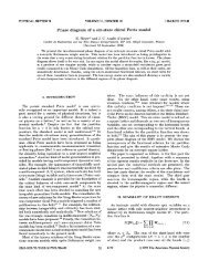
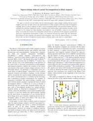
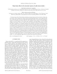
and release cycle. The results are reported<br />
in Fig. 1 and show the characteristic<br />
Stokes Raman spectrum observed in bulk<br />
silicon I under increasing hydrostatic<br />
pressures up to 16-18 GPa where a first<br />
phase transition occurs, presumably<br />
towards the Si II phase (body centred<br />
tetragonal, metallic), which has no sharp<br />
Raman response. After completion of the<br />
phase transition and transformation of all<br />
Si I into Si II, pressure is progressively<br />
released. This does not lead to Si I phase<br />
retrieval but instead, and like in the bulk<br />
material, Si II remains stable down to the<br />
5-10 GPa range where a phase transition<br />
towards Si III phase takes place. The<br />
characteristic Raman peaks of Si III are<br />
detected together with two broader bands<br />
corresponding to amorphous Si but no<br />
contribution from Si I is found. Upon<br />
aperture of the cell, as the pressure is<br />
fully released to room pressure, the<br />
alcohol evaporates and Si I phase is<br />
immediately recovered, without any<br />
transit via Si IV. This is most likeky due to<br />
the lack of heat sink in the wire<br />
surroundings and subsequent intense laser<br />
annealing of Si III. Further experiments<br />
are necessary to fully understand the<br />
diameter dependence of the phase<br />
transitions and special care will be given<br />
to the low-pressure domain upon pressure<br />
release where observation of the Si IV<br />
phase is expected.<br />
Fig. 1: Raman spectra obtained on a bundle of<br />
50 nm diameter Si NWs for increasing<br />
pressures (top) and decreasing pressures<br />
(bottom). The different phases are labeled I, II<br />
and III<br />
CONTACTS<br />
nicolas.pauc@cea.fr<br />
pierre.bouvier@grenoble-inp.fr<br />
mael.guennou@grenoble-inp.fr<br />
10<br />
HIGHLIGHT : NANOMATERIALS, NANOASSEMBLY AND NANOSTRUCTURATION