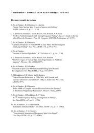
Activity Report 2010 - CNRS
Activity Report 2010 - CNRS
Activity Report 2010 - CNRS

You also want an ePaper? Increase the reach of your titles
YUMPU automatically turns print PDFs into web optimized ePapers that Google loves.
9 – TECHNOLOGICAL<br />
FACILITIES<br />
Created at the early stage of the<br />
Nanosciences Foundation in 2006, the<br />
“network of technological facilities”<br />
gathers most of the facilities concerned<br />
by nanofabrication, characterization at<br />
nanoscale, simulation and modeling of<br />
nanostructures, within the scientific area<br />
covered by the Foundation. The network<br />
is aimed to coordinate the financial<br />
support provided by the Foundation to<br />
the facilities. By supporting running costs<br />
of some facilities, the Foundation also<br />
eases the access to shared equipments.<br />
With almost 1/3 of its budget dedicated<br />
to the network of technological facilities,<br />
the Foundation contributes efficiently to<br />
the development of nanotechnologies<br />
involving physics, chemistry and biology.<br />
The facilities are opened to the whole<br />
community of researchers, post doctoral<br />
fellows and students involved in<br />
nanosciences. They offer state-of-the-art<br />
equipments for nanofabrication,<br />
nanocharacterisation and numerical<br />
simulation. More than 80% of the overall<br />
projects supported by the Foundation<br />
uses or have used the equipments of the<br />
network and many other national and<br />
European projects also benefits from<br />
them.<br />
THE NETWORK<br />
The network is composed by four<br />
facilities dedicated to:<br />
Nanofabrication<br />
Nanocharacterization<br />
Nano-chemistry and biology<br />
Numerical simulation<br />
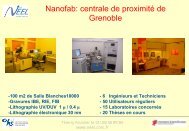
The Nanofabrication Facility<br />
This Nanofabrication facility covers 1000<br />
m 2 dispatched over two clean rooms<br />
located in close proximity. These clean<br />
rooms offer top level equipments for<br />
optical and electron beam lithography,<br />
metals and oxides deposition, reactive<br />
ion etching, chemical cleaning and<br />
etching, characterization and metrology.<br />
They are specially equipped to process<br />
samples of various sizes (from millimetre<br />
up to 4 inches). Special procedures have<br />
been implemented to avoid cross<br />
contamination as different types of<br />
materials (semiconductors, metals and<br />
polymers) can be processed in the<br />
facility. This flexibility is particularly<br />
important to provide a full access to the<br />
networks members.<br />
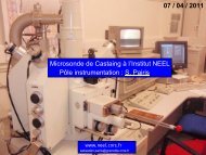
PTA:<br />
The Plateforme Technologique Amont<br />
(PTA) operated by CEA, <strong>CNRS</strong>, Grenoble<br />
INP and UJF and located on the MINATEC<br />
campus, provides to the community upto-date<br />
equipments for nanofabrication<br />
including electron beam lithography,<br />
etching (ion beams, reactive plasma) and<br />
deposition. The main topics developed in<br />
the PTA deal with nanoelectronics,<br />
spintronics, and photonics. Since 2009<br />
and thanks to the merger of PTA and<br />
CIME Nanotech clean rooms, the PTA<br />
provides also equipments dedicated to<br />
the fabrication of Micro-Electro<br />
Mechanical Systems (MEMS).<br />
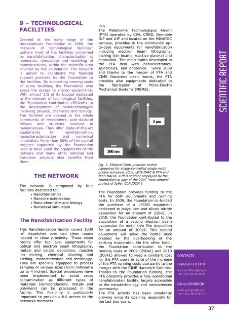
Fig. 1: Elliptical GaAs photonic etched<br />
nanowires for shape-controlled single mode<br />
photon emission. [Coll. LETI-INAC & PTA and<br />
Nitin MALIK, a PhD student employed by the<br />
Foundation as part of the 2007 “new comers”<br />
project of Julien CLAUDON.]<br />
The Foundation provides funding to the<br />
PTA for both equipments and running<br />
costs. In 2009, the Foundation co-funded<br />
the purchase of a LPCVD equipment<br />
dedicated to polysilicon and silicon nitride<br />
deposition for an amount of 220k€. In<br />
<strong>2010</strong>, the Foundation contributed to the<br />
acquisition of a second electron beam<br />
evaporator for metal thin film deposition<br />
for an amount of 300k€. This second<br />
equipment will solve the bottle neck<br />
created by the overbooking of the<br />
existing evaporator. On the other hand,<br />
the Foundation contribution to the<br />
running costs in 2009 (250k€) and <strong>2010</strong><br />
(200k€) allowed to keep a constant cost<br />
for the PTA users in spite of the increase<br />
of the PTA running costs due partly to the<br />
merger with the CIME Nanotech facilities.<br />
Thanks to the Foundation funding, the<br />
PTA presently provides a fully operational<br />
nanofabrication facility, largely accessible<br />
to the nanotechnology and nanosciences<br />
community.<br />
The PTA activity has been constantly<br />
growing since its opening, especially for<br />
the last two years.<br />
CONTACTS<br />
François LEFLOCH<br />
francois.lefloch@cea.fr<br />
Tel: +33 4 38 78 48 22<br />
Cécile GOURGON<br />
cecile.gourgon@cea.fr<br />
Tel: +33 4 38 78 98 37<br />
37<br />
SCIENTIFIC REPORT