Activity Report 2010 - CNRS
Activity Report 2010 - CNRS
Activity Report 2010 - CNRS

Create successful ePaper yourself
Turn your PDF publications into a flip-book with our unique Google optimized e-Paper software.
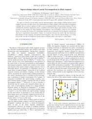
SCIENTIFIC REPORT<br />
FURTHER READING:<br />
J. Phys. D: Appl. Phys. 43 374008 (<strong>2010</strong>)<br />
Interface structure of graphene on SiC : an<br />
ab initio and STM approach<br />
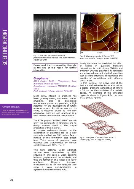
Fig. 2: Silicium nanowires used for<br />
photoluminescence studies (the scale marker<br />
equals 10 μm)<br />
Please read the corresponding Highlight<br />
at the end of this report for further<br />
information<br />
Graphene<br />
RTRA Project 2008 : “Graphene : from<br />
materials to test devices ”<br />
Coordinator: Laurence MAGAUD (Institut<br />
Néel)<br />
Post-doctoral Fellow: Vincent RENARD<br />
Since 2005, interest in graphene has<br />
been growing among condensed matter<br />
physicists, due to exceptional<br />
fundamental properties, promising a high<br />
potential for the development of future<br />
nanoelectronics. As silicon reaches its<br />
limits, it becomes crucial to find new<br />
alternative materials and graphene is a<br />
very serious candidate for that purpose.<br />
Fig. 3: Graphene on the C-face of SiC<br />
observed by AFM (sample grown in LMGP)<br />
Finally the team has modelled the effect<br />
of ripples in quantum transport<br />
calculations for both zigzag (ZGNR) and<br />
armchair (AGNR) graphene nanoribbons<br />
and extracted relevant physical quantities<br />
such as band structure, conductance and<br />
mobility of nanoribbons with different<br />
lateral width.<br />
In that purpose, the active part of the<br />
device is defined either by an armchair or<br />
a zigzag graphene nanoribbon of length<br />
≈ 20 nm, for the simulation of a realistic<br />
device. An example of the simulated<br />
ripples is shown in Figure 4 for the case<br />
of 1D and 2D ripples.<br />
The RTRA project “DISPOGRAPH” aims to<br />
unify the community in Grenoble and to<br />
design devices based on the unique<br />
properties of this material.<br />
An original endeavour focused on the<br />
elaboration of graphene led to a new<br />
synthesis method on SiC carbon face -<br />
instead of the commonly used silicon<br />
face. Thick layers of graphene were<br />
obtained and characterized by Raman<br />
spectroscopy and AFM. (Fig. 3)<br />
Thin films obtained under ultrahigh<br />
vacuum were characterized by STM,<br />
showing in this case a weak coupling<br />
between graphene and the substrate, and<br />
thus the formation of a quasi-ideal layer<br />
graphene. Magneto transport<br />
measurements at low temperatures also<br />
show a weak anti-localization in<br />
agreement with the theory WAL.<br />
Fig.4: Examples of nanoribbons with 1D<br />
ripples (up) and 2D ripples (down).<br />
20