Activity Report 2010 - CNRS
Activity Report 2010 - CNRS
Activity Report 2010 - CNRS

You also want an ePaper? Increase the reach of your titles
YUMPU automatically turns print PDFs into web optimized ePapers that Google loves.
SCIENTIFIC REPORT<br />
Exploring new concepts for<br />
photovoltaics with II-VI<br />
heterostructures<br />
Chair of Excellence 2009: Yong ZHANG<br />
Coordinator: Henri MARIETTE (Institut<br />
Néel)<br />
Thanks to their appropriate range of<br />
energy gaps, II-VI materials are already<br />
intensively used in solar cells.<br />
This novel project explores new concepts<br />
which are likely to improve the efficiency<br />
of II-VI solar cells and/or reduce their<br />
cost. Among the most promising ones<br />
figure type II band configurations, which<br />
favour the separation of photogenerated<br />
electron – hole pairs, and the nanowire<br />
geometry, which can be used to<br />
enhance light absorption and improve<br />
current collection.<br />
Promising first results have already been<br />
obtained along both lines. Noticeably,<br />
test planar CdSe/ZnTe heterostructures,<br />
grown by molecular beam epitaxy,<br />
display a three orders of magnitude<br />
enhancement of the lifetime of<br />
photogenerated carriers thanks to their<br />
type II band configuration.<br />
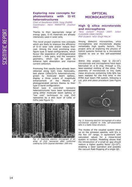
Novel type II core-shell nanowire<br />
heterostructures have been synthesized<br />
using either molecular beam epitaxy or<br />
“low cost” techniques to coat ZnO<br />
nanowires by a thin layer of CdSe or<br />
CdTe (see Figure 2).<br />
OPTICAL<br />
MICROCAVITIES<br />
High Q silica microtoroids<br />
and microspheres<br />
“New comers” Project 2007: Julien<br />
CLAUDON (INAC/SP2M)<br />
PhD student: Nitin Singh MALIK<br />
Among dielectric microcavities, silica<br />
microspheres and microtoroids display<br />
remarkably high quality factors. This<br />
project aims at exploring the physics of<br />
hybrid systems formed by a microtoroid<br />
coupled to one or few self-assembled<br />
QDs.<br />
Within this project, high Q (Q>10 7 )<br />
microtoroids and microspheres have been<br />
fabricated on a Si chip, through a CO 2<br />
laser-assisted melting of the silica. The<br />
assembly of microtoroids to tiny GaAs<br />
mesa structures containing InAs QDs has<br />
been realized for the first time in the<br />
RTRA dual beam FIB system, following a<br />
cut, pick and place procedure (see Figure<br />
3).<br />
µ-toroid<br />
Mesa<br />
Fig. 3: Scanning electron micrograph of a silica<br />
microtoroid coupled to InAs self-assembled<br />
QDs in a GaAs mesa structure.<br />
Fig. 2: Scanning electron micrograph of an<br />
array of ZnO nanowires after conformal<br />
coating by CdTe (typical diameter: 200 nm)<br />
The modes of the coupled system show<br />
up on the emission spectra, with Q’s in<br />
the few 10 3 range, in agreement with<br />
calculated values for a mesa-toroid<br />
system in contact. Modelling shows that<br />
the introduction of a small air gap should<br />
restore a higher quality factor (Q>10 5 ),<br />
enabling a laser operation and possibly<br />
the vacuum Rabi-flopping of a single QD.<br />
14