Activity Report 2010 - CNRS
Activity Report 2010 - CNRS
Activity Report 2010 - CNRS

Create successful ePaper yourself
Turn your PDF publications into a flip-book with our unique Google optimized e-Paper software.
when compared, for example, to the<br />
prototype of the US “competitor” project<br />
MUSIC (to be installed at the CSO 10-m<br />
sub-mm observatory in Mauna Kea, and<br />
being developed years before NIKA).<br />
MUSIC involves laboratories like Caltech,<br />
JPL, University of Santa Barbara and<br />
others.<br />
A second week technical time on the<br />
IRAM telescope was approved in October<br />
<strong>2010</strong>. The sensitivity of the LEKID array<br />
improved by a factor of three compared<br />
to the first run in 2009, verifying that<br />
NIKA is rapidly approaching the final<br />
target of sensitivity.<br />
This second run was a total success,<br />
allowing the observation, for example, of<br />
a large number of extended sources.<br />
Please read the corresponding Highlight<br />
at the end of this report for further<br />
information.<br />
group at Université Catholique de<br />
Louvain-Louvain-la-Neuve. The upgrading<br />
of the SGM tool is the main activity of a<br />
shared PhD student hired by the<br />
foundation (Peng LIU).<br />
InGaAs/InAlAs heterostructures are<br />
grown by Molecular Beam Epitaxy at<br />
IEMN (Lille) and patterned by e-beam<br />
lithography at UCL for obtaining Quantum<br />
Rings. The results are interpreted thanks<br />
to quantum conductance simulations<br />
performed at IMEP (Grenoble) by Marco<br />
Pala.<br />
SCIENTIFIC REPORT<br />
Scanning<br />
gate<br />
Nanoelectronics<br />
Chair of Excellence 2007: Vincent BAYOT<br />
Coordinators: Hervé COURTOIS and<br />
Serge HUANT (Institut Néel).<br />
In the framework of Vincent Bayot’s Chair<br />
of Excellence, two major results were<br />
obtained by Scanning Gate Microscopy<br />
(SGM) :<br />
a theoretical understanding of SGM<br />
images in the coherent regime of<br />
transport both in the presence of<br />
defects and weak magnetic field<br />
the discovery of Coulomb islands in a<br />
Quantum Hall (QH) interferometer.<br />
In the latter, SGM was used for obtaining<br />
a spatially resolved investigation of<br />
electron transport inside an<br />
interferometer formed by an<br />
InGaAs/InAlAs Quantum Ring (QR),<br />
driven in the integer QH regime. The<br />
pseudo Aharonov–Bohm (AB) period was<br />
associated with a specific Coulomb island<br />
formed by edge state loops enclosing a<br />
hill or a valley in the potential. Each<br />
active Coulomb island was located<br />
precisely inside the QR by tuning the<br />
magnetic field and imaging the spatial<br />
shift of Coulomb resonances by means of<br />
SGM.<br />
The (SGM) uses the electrically polarized<br />
tip of a low-temperature AFM to scan<br />
above a semiconductor device and record<br />
the change in conductance at point (x,y),<br />
induced by the tip located at that point.<br />
The SGM tool is being developed jointly<br />
at the Institut Néel by the group of Serge<br />
HUANT and Hermann SELLIER in<br />
collaboration with Vincent BAYOT and his<br />
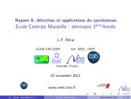
Fig. 3: Vincent BAYOT, Chair of Excellence in<br />
2007<br />
Please read the corresponding Highlight<br />
at the end of this report for further<br />
information.<br />
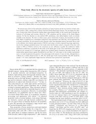
Superconducting<br />
Nanostructures<br />
Chair of Excellence 2009: John R.<br />
KIRTLEY<br />
Coordinator: Klaus HASSELBACH (Institut<br />
Néel).<br />
John R. KIRTLEY is one of the world’s<br />
leading experts on Josephson junction<br />
devices and superconductivity. The<br />
project is aimed at the study of the<br />
physical properties of high quality<br />
superconducting films and their<br />
integration into quantum nano-devices.<br />
First results have been obtained in <strong>2010</strong>.<br />
As a matter of fact the core of a<br />
conventional tunnel barrier is formed of<br />
oxidized nano-grains with fluctuating<br />
electric charges at their surface. These<br />
charges are suspected of causing<br />
decoherence of superconducting Qbits.<br />
Thanks to molecular beam epitaxy a<br />
charge-free junction was achieved by<br />
growing epitaxial layers of Rhenium /<br />
Sapphire / Rhenium (Re/Al 2 O 3 /Re), giving<br />
a superconducting Qubit. The layers have<br />
been grown successfully by the group of<br />
B. Gilles (SIMAP), on sapphire substrates,<br />
and characterized by STM, AFM and X-ray<br />
diffraction.<br />
FURTHER READING<br />
Nat. Commun. 1:39, (<strong>2010</strong>)<br />
Imaging Coulomb islands in a quantum<br />
Hall interferometer<br />
Nanotechnology, 20, 264021 (2009)<br />
Scanning gate microscopy of quantum<br />
rings: effects of an external magnetic<br />
field and of charged defects.<br />
25