Activity Report 2010 - CNRS
Activity Report 2010 - CNRS
Activity Report 2010 - CNRS

You also want an ePaper? Increase the reach of your titles
YUMPU automatically turns print PDFs into web optimized ePapers that Google loves.
SCIENTIFIC REPORT<br />
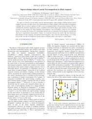
Fig. 5: Tunneling FET operating principle and schematics of the device. The TFET is made out a<br />
gated PN diode: when the gate is biased at 0, no carrier can flow from drain to source because of<br />
the wide tunnel barrier they have to flow through. But when the gate voltage is decreased the<br />
barrier width is narrowed down allowing for band to band tunneling current.<br />
FURTHER READING:<br />
Appl. Phys. Lett. 94, 263508 (2009)<br />
Tunneling field-effect transistor with<br />
epitaxial junction in thin germanium-oninsulator<br />
Microelectronic Engineering (2011)<br />
Gate-induced drain leakage in FD-SOI<br />
devices: What the TFET teaches us about the<br />
MOSFET<br />
6<br />
Tunneling-based nano-FETs<br />
Chair of Excellence 2008: Alex<br />
ZASLAVSKY<br />
Coordinator: Sorin CRISTOLOVEANU<br />
(IMEP-LAHC).<br />
The objective of this project is to<br />
investigate the technological potential of<br />
tunneling FETs (TFETs) built in<br />
semiconductor-in-insulator technology to<br />
complement or possibly replace standard<br />
CMOS FETs in digital logic circuits. These<br />
TFETs are theoretically predicted to<br />
manifest sharper on-off characteristics<br />
and higher I ON currents than Si<br />
CMOSFETs.<br />
If this theoretical promise is confirmed,<br />
the technological insertion of such<br />
devices is likely in the longer term, when<br />
hybrid systems combining standard<br />
CMOS logic with islands of alternative<br />
technologies become standard. Also TFET<br />
devices provide an experimental testbed<br />
for interband tunneling (and other<br />
quantum effects).<br />
So far experimental demonstrations have<br />
not fulfilled the theoretical expectations.<br />
The originality of the approach of this<br />
project is to combine advanced<br />
technological fabrication with solid<br />
modeling and characterization.<br />
A emphasis is put on the comparison of<br />
germanium-on-insulator (GeOI) TFETs<br />
with their silicon-on-insulator (SOI)<br />
counterparts in order to address high on<br />
currents. Indeed there have been<br />
already several reports of sub-60<br />
mV/decade subthreshold slope in SOI<br />
TFETs (including a world-leading result<br />
from LETI-CEA) but at the expense of<br />
relatively low I ON due to the large<br />
bandgap of Si and insufficiently abrupt<br />
junctions. Conversely, GeOI TFETs are<br />
expected to have considerably larger I ON .<br />
The project has already allowed to<br />
experimentally demonstrate theoretical<br />
calculations: interest of HfO 2 as high k<br />
gate dielectric in order to improve the<br />
subthreshold slope, interest of Ge to<br />
increase the on current… The project has<br />
lead to 3 publications in <strong>2010</strong> (ESSDERC,<br />
JAP and APL) and some patents are<br />
pending.<br />
Fig.6: Alex ZASLAVSKY, Chair of Excellence<br />
2008