Activity Report 2010 - CNRS
Activity Report 2010 - CNRS
Activity Report 2010 - CNRS

You also want an ePaper? Increase the reach of your titles
YUMPU automatically turns print PDFs into web optimized ePapers that Google loves.
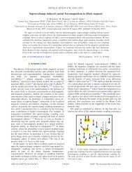
HIGHLIGHT : QUANTUM NANOELECTRONICS<br />
CONTACTS<br />
laurent.duraffourg@cea.fr<br />
philippe.andreucci@cea.fr<br />
roukes@caltech.edu<br />
FURTHER READING<br />
R. B. Karablin et al, Applied Physics Letters,<br />
95, 103111, (2009)<br />
E. Mile et al, Nanotechnology, 21, 165504<br />
(<strong>2010</strong>)<br />
1<br />
NANO-<br />
ELECTROMECHANICAL<br />
RESONATORS<br />
The Chair of Excellence of Michael<br />
ROUKES aims to merge advances in<br />
nanotechnology with very-large-scale<br />
integration (VLSI) processes in order to<br />
create complex nanomechanical systemsbased<br />
tools for science and industry—<br />
thus accelerating nanoscience out of the<br />
laboratory and into the marketplace.<br />
The emerging field of<br />
nanoelectromechanical systems (NEMS)<br />
is attracting considerable interest. These<br />
miniaturized nanoscale devices,<br />
particularly cantilever and beam flexuralmode<br />
resonators, have enabled the<br />
demonstrations of single molecule mass<br />
sensors and single cell level-force<br />
sensors. The small displacements of<br />
these miniaturized devices induce very<br />
low signals which are overwhelmed by<br />
parasitic background. A lot of efforts<br />
have been devoted to developing new<br />
transduction and background reduction.<br />
Piezoelectric and piezoresistive<br />
transductions appear to be particularly<br />
advantageous compared to the more<br />
conventionally employed magnetomotive<br />
and capacitive techniques.<br />
Amongst the attributes of chosen<br />
transduction, principles are intrinsic<br />
integrability, high efficiency and electrical<br />
tunability, low power consumption, and<br />
low thermal budgets for materials<br />
processing, permitting post-CMOS<br />
integration.<br />
Silicon nanowire<br />
piezoresistive detection<br />
A piezoresistive detection scheme offers<br />
great potential compared to a capacitive<br />
one especially for high resonant<br />
frequency measurements. Recently, mass<br />
resolution down to 7 zeptograms Hz 1/2 has<br />
been demonstrated using a metallic<br />
gauge layer deposited on the top of a<br />
cantilever. Another approach consists in<br />
using a doped silicon nanowire. However<br />
to date bottom-up nanowires cannot be<br />
fabricated using a VLSI process<br />
compatible with a standard CMOS<br />
technology.<br />
We demonstrate a new kind of detection<br />
scheme based on doped silicon nanowire<br />
strain gauges that are fully compatible<br />
with CMOS processes. This allows very<br />
large scale integration of devices in a<br />
straightforward manner. Measurements<br />
obtained with this approach are showing<br />
promising performances in terms of<br />
frequency stability, dynamic range, and<br />
achievable mass resolution (Fig.1).<br />
Fig. 1: Nano cantilever beam resonator based<br />
on silicon nanowire piezoresistive detection –<br />
Very large signal to noise ratio<br />
The devices tested in this work were<br />
developed as prototypes and were not<br />
optimized for mass detection at this<br />
stage. Such NEMS have a great potential<br />
for future performance improvements<br />
and new applications opportunities.<br />
Further device optimization for lower<br />
mass and higher frequency, based on<br />
advanced top-down nanowire fabrication<br />
techniques (for instance 40nm-silicon<br />
thickness), will lead to a resolution in the<br />
range of a few zeptograms or less.<br />
Piezoelectric<br />
nanoelectromechanical<br />
resonators<br />
We also demonstrated piezoelectrically<br />
actuated, electrically tunable NEMS based<br />
on multilayers containing a 100-nm-thin<br />
aluminum nitride (AlN) layer. Efficient<br />
piezoelectric actuation of very high<br />
frequency fundamental flexural modes up<br />
to 80 MHz has been demonstrated at<br />
room temperature (Fig.2).<br />
Fig. 2: Very High Frequency AlN beam<br />
resonators demonstrating nonlinearity (a) and<br />
frequency tuning behaviour (b).<br />
To conclude, 11 patents were deposited.<br />
Moreover an Alliance for Nanosystems<br />
VLSI between Caltech/KNI and Léti-<br />
Minatec was created thanks to the<br />
support of the Nanosciences Foundation.