Activity Report 2010 - CNRS
Activity Report 2010 - CNRS
Activity Report 2010 - CNRS

You also want an ePaper? Increase the reach of your titles
YUMPU automatically turns print PDFs into web optimized ePapers that Google loves.
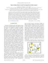
HIGHLIGHT : NANOPHOTONICS<br />
CONTACTS<br />
julien.claudon@cea.fr<br />
FURTHER READING<br />
J. Claudon et al. Nature Photonics, 4,<br />
p174, (<strong>2010</strong>)<br />
J. Bleuse et al, Phys. Rev. Lett, 106,<br />
103601 (2011)<br />
5<br />
A BRIGHT SINGLE-<br />
PHOTON SOURCE<br />
BASED ON A PHOTONIC<br />
NANOWIRE<br />
The realization of an efficient, on-demand<br />
single-photon source (SPS) is an<br />
important goal for the development of<br />
quantum cryptography and photonic<br />
quantum information processing. In this<br />
context, semiconductor quantum dots<br />
(QD) are very attractive: at low<br />
temperature, they offer a stable singlephoton<br />
emission with a nearly perfect<br />
radiative yield. However, they are<br />
generally embedded in a high index<br />
semiconductor matrix that prevents the<br />
efficient collection of light in the far field.<br />
Within the “Strongchip” young scientist<br />
project supported by the Nanoscience<br />
Foundation, we have overcome this<br />
limitation and demonstrated a very bright<br />
SPS by inserting the QD inside a novel,<br />
well controlled electromagnetic<br />
environment: a photonic nanowire.<br />
A photonic wire is a monomode optical<br />
waveguide that is made of a high index<br />
dielectric material. Specifically, we<br />
consider here a structure defined in III-<br />
As semiconductors and shown in Fig. 1:<br />
the wire is made of GaAs (n=3.5) and is<br />
surrounded by air (n=1). It contains an<br />
InAs QD whose fundamental optical<br />
transition emits single photons at a free<br />
space wavelength around 920 nm. The<br />
high refractive index contrast between<br />
the wire and the air cladding has two<br />
important consequences. First, the<br />
guided mode is confined very tightly<br />
inside a wire having a 200 nm diameter,<br />
which guarantees a good coupling to the<br />
emitter. In addition, the coupling to the<br />
continuum of non-guided modes is<br />
strongly inhibited, thanks to a<br />
pronounced dielectric screening effect. As<br />
a consequence, the spontaneous<br />
emission of the QD is nearly completely<br />
funneled into the guided mode. Next, one<br />
has to collect efficiently the guided<br />
photons with a microscope objective<br />
located above the wire. For this goal, the<br />
two ends of the wire are carefully<br />
engineered. The photons emitted<br />
downward are reflected back into the<br />
guided mode with an integrated mirror,<br />
made of gold and silica. The upper wire<br />
end features a conical tip, designed to<br />
deconfine progressively the guided mode<br />
into the air cladding, in order to obtain a<br />
more directive far-field emission pattern.<br />
The fabrication process of such devices<br />
starts from a planar structure grown by<br />
molecular beam epitaxy. After deposition<br />
of the SiO 2 -Au mirror and a flip-chip step,<br />
the photonic nanowires are obtained with<br />
a dry plasma etching. Because it defines<br />
the nanowire geometry, this last step is<br />
critical and was carefully optimized.<br />
The sample was then mounted in a<br />
micro-photoluminescence setup and<br />
cooled down to liquid helium<br />
temperature. The injection of electronhole<br />
pairs to excite the QD luminescence<br />
was provided by a pulsed laser. The<br />
source efficiency, defined as the<br />
probability to emit a photon into the<br />
collecting cone of the microscope<br />
objective after an excitation pulse,<br />
reaches a maximum when the emitter is<br />
saturated. In these conditions, a record<br />
value of 0.72 photon per pulse was<br />
obtained. Simultaneously, intensity<br />
correlation measurements have provided<br />
the unambiguous signature of a very<br />
pure single-photon emission (g (2)