Activity Report 2010 - CNRS
Activity Report 2010 - CNRS
Activity Report 2010 - CNRS

You also want an ePaper? Increase the reach of your titles
YUMPU automatically turns print PDFs into web optimized ePapers that Google loves.
Growth, patterning, defects<br />
& structure of nano-objects.<br />
The elaboration and characterisation of<br />
nano-objects is of primary importance in<br />
nanosciences and requires a mastering of<br />
complex experimental methods.<br />
Numerical simulation is of great help in<br />
understanding the details of the physical<br />
mechanism involved in elaboration<br />
procedure and in interpreting the output<br />
of methods used to analyze the structure<br />
of these objects.<br />
In this context the Nanosciences<br />
Foundation supports so far three Chairs<br />
of Excellence and one PhD student.<br />
Chair of Excellence 2009: Normand<br />
MOUSSEAU<br />
Coordinator: Pascal POCHET<br />
(INAC/SP2M)<br />
This project started in early <strong>2010</strong>. It aims<br />
at coupling a kinetic method (k-ART)<br />
developed by Pr MOUSSEAU and the abinitio<br />
code BigDFT developed initially at<br />
INAC. The new methodology will then be<br />
coupled to study the growth of three<br />
types of nanostructures: SiGe quantum<br />
dots, Si nanowires and graphene on SiC.<br />
The first tests of the new methodology<br />
have already been done on the simpler<br />
system consisting of a fullerene C20.<br />
The goal of this project is therefore to<br />
benefit from the expertise of Pr Graves in<br />
the field of MDS applied to plasmasurface<br />
interactions to assist the fast<br />
development of etching processes of<br />
graphene layers.<br />
“Fil de l’eau” PhD student 2008: Arpan<br />
Krishna DEB<br />
Thesis Director: Thierry DEUTSCH and<br />
Damien CALISTE (INAC/SP2M).<br />
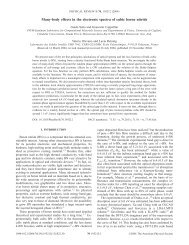
This thesis deals with cluster approach to<br />
simulate defects in Si or Ge. Indeed<br />
working with charged periodic systems is<br />
a bit complicated as it involves the long<br />
range Coulomb forces and it is impossible<br />
to negate the interaction between the<br />
images created due to the periodicity in<br />
the simulation. A very common approach<br />
is to add a neutralizing background<br />
charge. But even this trick does not<br />
completely eliminate the spurious<br />
interaction of the image charges. The<br />
cluster approach clearly avoids these<br />
difficulties and open new possibilities to<br />
treat these defects.<br />
SCIENTIFIC REPORT<br />
Chair of Excellence <strong>2010</strong>: David GRAVES<br />
Coordinator: Gilles CUNGE (LTM).<br />
The Chair of Excellence of Pr GRAVES<br />
(University of California at Berkeley) will<br />
deal with Nanometer Scale Control of<br />
Graphene Processing with Innovative<br />
Plasma Technology (NSCGP). This project<br />
aims to advance nanometer-scale control<br />
of graphene processing using advanced,<br />
innovative plasma technology. In order to<br />
exploit the extraordinary power of plasma<br />
for large area, smooth and damage-free<br />
graphene film growth and patterning, it<br />
will be necessary to take a leap in plasma<br />
technology.<br />
LTM is currently investing such a new<br />
technology: pulsed plasmas. However,<br />
the interactions between reactive<br />
plasmas and surfaces are so complex<br />
that the efficient development of<br />
processes for new materials requires<br />
numerical simulations.<br />
For 20 years, Molecular Dynamic<br />
Simulations (MDS) have proved to be<br />
powerful for this purpose, but this<br />
expertise does not exist locally.<br />
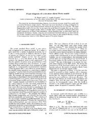
Fig. 5: Cluster of Si used for the simulation of<br />
a defect. Left: cluster with no defect inside.<br />
Right: cluster with one vacancy<br />
.<br />
35